

Preparation method for side gating graphene field effect transistor
A field-effect transistor and graphene technology, which is applied in semiconductor/solid-state device manufacturing, gaseous chemical plating, coating, etc., can solve the problems of improving the transconductance of field-effect transistors, easily destroying graphene, and expensive SiC wafers. Achieve the effect of improving modulation ability and avoiding adverse effects
- Summary
- Abstract
- Description
- Claims
- Application Information
AI Technical Summary
Problems solved by technology
Method used
Image


Examples
Embodiment 1
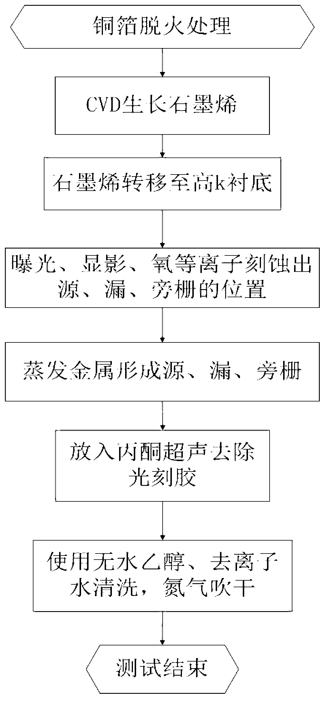
[0028] The realization steps of the present invention are as follows:
[0029] Step 1: Put the copper foil into the reaction chamber, and the reaction chamber is evacuated until the pressure is lower than 0.01 Pa. H was introduced into the reaction chamber with a flow rate of 10 sccm 2 , raise the temperature in the reaction chamber to 900°C, and perform thermal annealing on the copper foil, the annealing time is 60min;
[0030] Step 2: feed flow into reaction chamber as H of 50 sccm and CH of 10 sccm, grow graphene by chemical vapor deposition CVD for 15 min;
[0031] Step 3: After the reaction chamber is naturally cooled to room temperature, the growth sample is taken out, and polymethyl methacrylate PMMA is spin-coated on the graphene surface to form a laminated structure sample of copper foil-graphene-PMMA;
[0032] Step 4: Air-dry the laminated structure sample of the copper foil-graphene-PMMA, then make the PMMA face up to float in the concentration of 60g / L (NH 4 ) ...
Embodiment 2
[0039] The realization steps of the present invention are as follows:
[0040] Step A: Put the copper foil into the reaction chamber, and the reaction chamber is evacuated until the pressure is lower than 0.01 Pa. Introduce H2 with a flow rate of 15 sccm into the reaction chamber, raise the temperature in the reaction chamber to 950°C, and perform thermal annealing on the copper foil for 40 minutes;
[0041] Step B: feed into the reaction chamber H2 with a flow rate of 100 sccm and CH with a flow rate of 15 sccm, and grow graphene by chemical vapor deposition CVD for 10 min;
[0042] Step C: After the reaction chamber is naturally cooled to room temperature, the growth sample is taken out, and polymethyl methacrylate PMMA is spin-coated on the graphene surface to form a laminated structure sample of copper foil-graphene-PMMA;
[0043] Step D: air-dry the laminated structure sample of described copper foil-graphene-PMMA, then make PMMA face up and float in the (NH 4 ) 3 (S ...
Embodiment 3
[0050] The realization steps of the present invention are as follows:
[0051] Step 1: Put the copper foil into the reaction chamber, and the reaction chamber is evacuated until the pressure is lower than 0.01 Pa. Introduce H2 with a flow rate of 20 sccm into the reaction chamber, raise the temperature in the reaction chamber to 1000°C, and perform thermal annealing on the copper foil for 20 minutes;
[0052] Step 2: Introduce H into the reaction chamber with a flow rate of 200 sccm 2 and CH at a flow rate of 20 sccm 4 , grow graphene by chemical vapor deposition CVD for 10 minutes;
[0053] Step 3: After the reaction chamber is naturally cooled to room temperature, the growth sample is taken out, and polymethyl methacrylate PMMA is spin-coated on the graphene surface to form a laminated structure sample of copper foil-graphene-PMMA;
[0054] Step 4: air-dry the laminated structure sample of described copper foil-graphene-PMMA, then make PMMA face up and float in the (NH 4...
PUM
 Abstract
Description
Claims
Application Information