Method for growing high-quality semiconductor single-walled carbon nanotube through in-situ weak hydrogen etching

A single-walled carbon nanotube, semiconducting technology, applied in the field of hydrogen in-situ weak etching to grow high-quality semiconducting single-walled carbon nanotubes, can solve the problem of damage to the intrinsic structure of single-walled carbon nanotubes, the introduction of impurities, and cumbersome steps and other issues, to achieve the effect of good industrial application prospects, low cost, and easy scale

Active Publication Date: 2013-04-03
INST OF METAL RESEARCH - CHINESE ACAD OF SCI
View PDF1 Cites 15 Cited by
  • Summary
  • Abstract
  • Description
  • Claims
  • Application Information

AI Technical Summary

Problems solved by technology

[0006] A technical problem solved by the present invention is to overcome the problems such as cumbersome steps in the current preparation and separation process, high cost, and serious damage to the intrinsic structure of single-walled carbon nanotubes; another technical problem solved by the present invention is to overcome Solve the existing problems such as low output, large loss, and introduction of impurities in the existing method of directly preparing semiconducting single-walled carbon nanotubes

Method used


Image

  • Method for growing high-quality semiconductor single-walled carbon nanotube through in-situ weak hydrogen etching
  • Method for growing high-quality semiconductor single-walled carbon nanotube through in-situ weak hydrogen etching
  • Method for growing high-quality semiconductor single-walled carbon nanotube through in-situ weak hydrogen etching

Examples


Embodiment 1

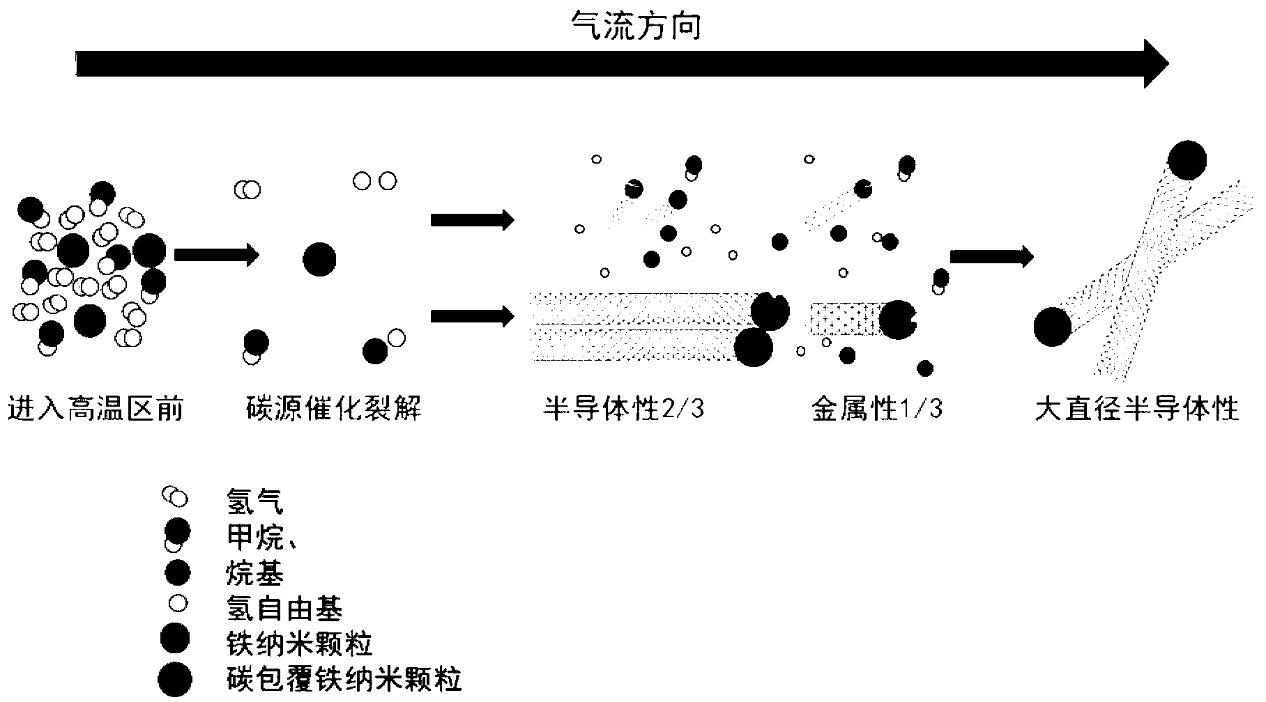
[0035] (1) figure 1 In order to prepare a schematic diagram of the principle of high-quality, semiconducting single-walled carbon nanotubes, the specific experimental steps are as follows: a piece of ferrocene containing sulfur powder (the weight ratio of sulfur powder to ferrocene is 1:200) is placed in the chemical vapor deposition In the low-temperature zone of the reaction furnace (50mm in diameter, 10cm in length of the constant temperature zone), the temperature rises to 1100°C at a rate of 22°C / min under a hydrogen atmosphere, and 30ml / min of methane is introduced, and the flow rate of hydrogen is adjusted to 2000ml / min. min, and at the same time push the ferrocene to a furnace with a temperature of 80° C. to grow single-walled carbon nanotubes for 30 minutes. After the chemical vapor deposition is finished, turn off the methane, and reduce the hydrogen flow rate to 400ml / min, allowing the reaction furnace to cool down to room temperature naturally.

[0036] (2) The sa...

Embodiment 2

[0046] (1) Place a piece of nickelocene containing sulfur powder (the weight ratio of sulfur powder to nickelocene is 1:100) in the low temperature zone of the chemical vapor deposition reaction furnace (50mm in diameter, 10cm in length of the constant temperature zone). Under the hydrogen atmosphere, the temperature was raised to 1100°C at a rate of 22°C / min, and 20ml / min of methane was introduced, and the flow rate of hydrogen was adjusted to 2300ml / min. For the growth of walled carbon nanotubes, the growth time was 40 minutes. After the chemical vapor deposition is over, turn off the methane, and reduce the hydrogen flow rate to 400ml / min again, and allow the reaction furnace to cool down to room temperature by natural cooling.

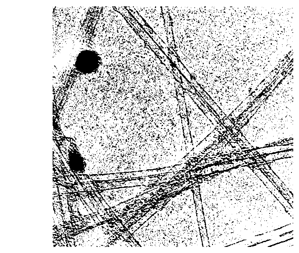
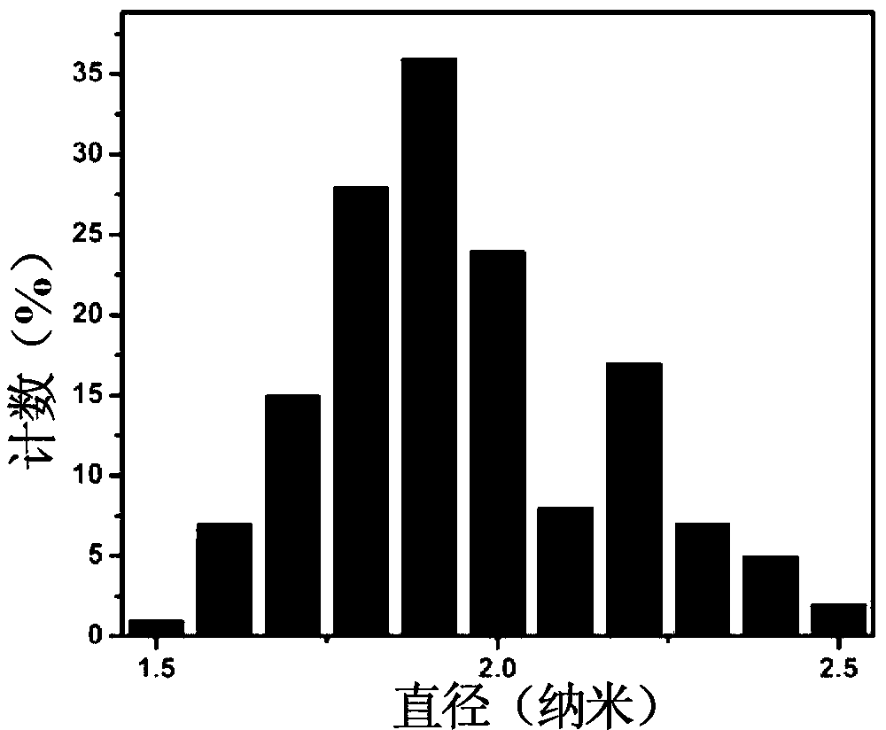
[0047] (2) The samples obtained in step (1) were characterized by transmission electron microscope, Raman spectrum and absorption spectrum respectively. The diameters of 146 single-walled carbon nanotubes were measured and counted under a transmis...

Embodiment 3

[0050](1) Place a piece of cobaltocene containing sulfur powder (the weight ratio of sulfur powder to cobaltocene is 1:150) in the low temperature zone of a chemical vapor deposition reaction furnace (50mm in diameter, 10cm in length of the constant temperature zone), in the Under a hydrogen atmosphere, the temperature was raised to 1050°C at a rate of 22°C / min, 25ml / min of ethylene was introduced, and the hydrogen flow rate was adjusted to 2500ml / min. For the growth of walled carbon nanotubes, the growth time was 50 minutes. After the chemical vapor deposition is finished, turn off ethylene, reduce the hydrogen flow rate to 400ml / min, and allow the reaction furnace to cool down to room temperature naturally.

[0051] (2) The samples obtained in step (1) were characterized by transmission electron microscope, Raman spectrum and absorption spectrum respectively. The diameters of 132 single-walled carbon nanotubes were measured and counted under the transmission electron micros...


PUM

PropertyMeasurementUnit
diameteraaaaaaaaaa
anti-oxidation temperatureaaaaaaaaaa
diameteraaaaaaaaaa

Abstract

The invention relates to the field of fabrication of a high-quality semiconductor single-walled carbon nanotube, in particular to a method for directly growing the high-quality semiconductor single-walled carbon nanotube through in-situ weak hydrogen etching. A metallic and small-diameter single-walled carbon nanotube can be etched in situ at a certain reaction temperature by regulating and optimizing a flow of carrier gas, namely hydrogen and under the conditions of taking dicyclopentadienyl iron as a catalyst precursor, sulfur powder as a growth promoter and organic low-carbon hydrocarbon as a carbon source; and the high-quality semiconductor-superior single-walled carbon nanotube is finally obtained. The content of the semiconductor single-walled carbon nanotube is greater than or equal to 91wt%, the diameter distribution is between 1.5nm and 2.5nm, and the highest concentrated oxidation temperature reaches 800 DEG. With the adoption of the method, the massive, fast and low-cost controlled growth of the semiconductor single-walled carbon nanotube with the narrower diameter distribution and the high quality is realized, and the problems such as serious damages to a sample due to a strong etching agent, complexity of a fabrication process, low output and high cost during a selective fabrication course of a conduction-superior single-walled carbon nanotube can be effectively solved.

Description

technical field [0001] The invention relates to the field of direct, massive and controllable preparation of high-quality semiconducting single-walled carbon nanotubes, specifically a method for directly growing high-quality semiconducting single-walled carbon nanotubes by hydrogen in-situ weak etching, which is used in floating catalyst chemistry In the process of growing single-walled carbon nanotubes by vapor deposition, the flow rate of carrier gas and etching gas-hydrogen is adjusted in situ, and the macroscopic and controllable growth of semiconducting single-walled carbon nanotubes with narrow diameter distribution is realized. Background technique [0002] Single-walled carbon nanotubes are formed by curling a single layer of graphene around a certain vector, and according to the chirality and diameter, single-walled carbon nanotubes can be divided into metallic or semiconducting single-walled carbon nanotubes. Due to the excellent electron transport properties of si...

Claims


Application Information

Patent Timeline
Patent Type & Authority Applications(China)
IPC IPC(8): C01B31/02B82Y40/00C01B32/159C01B32/162
Inventor 侯鹏翔李文山刘畅成会明
Owner INST OF METAL RESEARCH - CHINESE ACAD OF SCI
Why Eureka
Try Eureka