High-voltage inverted LED chip and manufacturing method thereof

A technology for LED chips and manufacturing methods, applied in electrical components, circuits, semiconductor devices, etc., can solve the problem of limited process line width, inability to overcome differences in bump size, welding uniformity and flatness, yield problems, high difficulty, etc. question

Inactive Publication Date: 2013-04-03
ENRAYTEK OPTOELECTRONICS
View PDF6 Cites 35 Cited by
  • Summary
  • Abstract
  • Description
  • Claims
  • Application Information

AI Technical Summary

Problems solved by technology

Due to the use of bump welding technology, it cannot overcome the yield problems caused by the difference in bump size, welding uniformity and flatness, etc. The process is complicated and the reliability is low.
[0005] In the Chinese patent application with application number 201110296263.8, another method for manufacturing high-voltage LED chips is disclosed, which uses ICP deep etching to make isolation trench...

Method used


Image

  • High-voltage inverted LED chip and manufacturing method thereof
  • High-voltage inverted LED chip and manufacturing method thereof
  • High-voltage inverted LED chip and manufacturing method thereof

Examples


Embodiment Construction

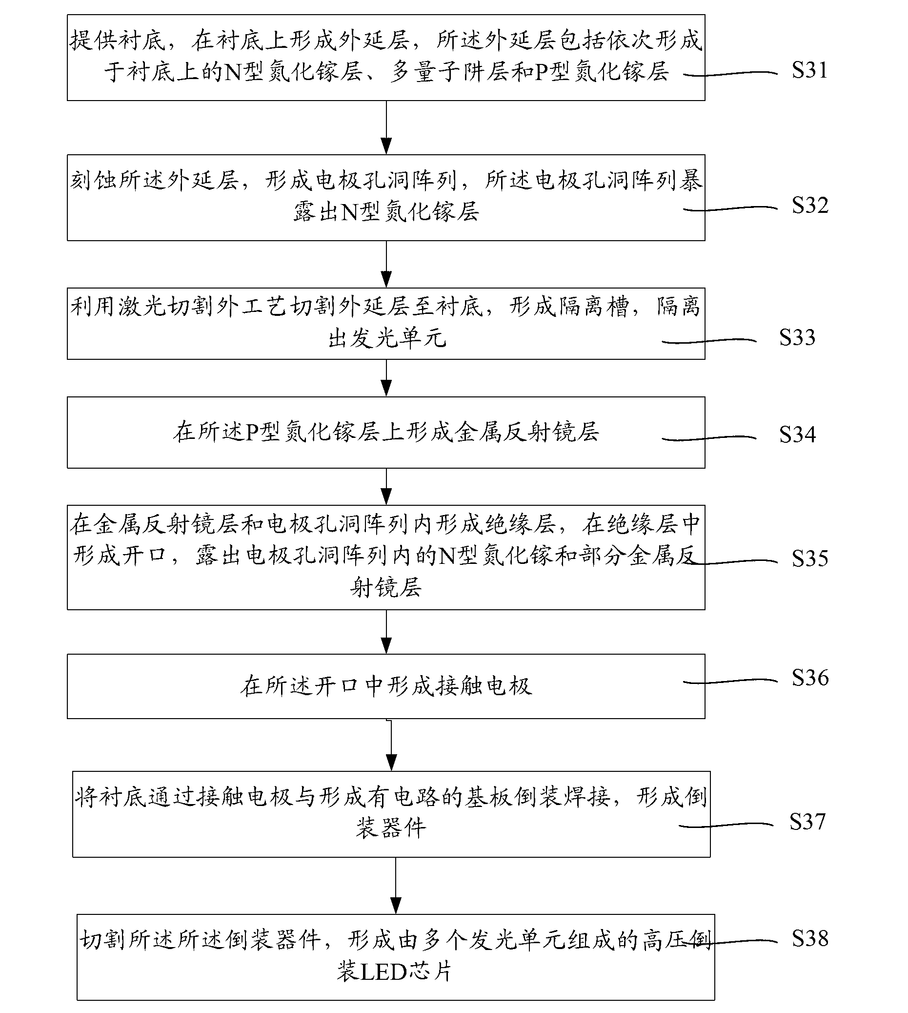
[0031] As mentioned in the background technology, on the one hand, the existing high-voltage flip-chip LED chips use bump welding technology, and the bump welding technology has its own process defects; on the other hand, the formation of the isolation trench of the light-emitting unit has process limitations , easy to sacrifice a large amount of light-emitting area.

[0032] To this end, the present invention provides a method for manufacturing a high-voltage flip-chip LED chip. The method for manufacturing a high-voltage flip-chip LED chip optimizes the process of the existing high-voltage flip-chip LED chip, avoids bump welding technology, and simultaneously The laser cutting technology is used to isolate the light emitting unit, and the process is simple and avoids sacrificing too much light emitting area.

[0033] The present invention will be described in more detail below with reference to the accompanying drawings, wherein preferred embodiments of the present invention...


PUM

PropertyMeasurementUnit
Thicknessaaaaaaaaaa
Thicknessaaaaaaaaaa

Abstract

The invention discloses a high-voltage inverted LED chip and a manufacturing method thereof. The manufacturing method of the LED chip includes: etching an epitaxial layer to form an electrode hole array; cutting the epitaxial layer to a substrate by means of the laser cutting technique to form isolation grooves to isolate luminous units; forming a metal reflector layer on a P-type gallium nitride layer; forming an insulating layer in the metal reflector layer and the electrode hole array and forming an opening in the insulating layer to expose part of the metal reflector layer and N-type gallium nitride in the electrode hole array; forming a contact electrode in the opening; welding the substrate and a base plate on which a circuit is formed in an inverted manner through the contact electrode to form an inverted device; and cutting the inverted device to form the high-voltage inverted LED chip consisting of multiple luminous units. The high-voltage inverted LED chip and the manufacturing method thereof have the advantages of simple process and high device reliability.

Description

technical field [0001] The invention relates to the technical field of LED manufacturing, in particular to a high-voltage flip-chip LED chip and a manufacturing method thereof. Background technique [0002] Light Emitting Diode (LED, Light Emitting Diode) is a semiconductor solid-state light-emitting device that uses a semiconductor PN junction as a light-emitting material to convert electricity into light. When a forward voltage is applied to both ends of the semiconductor PN junction, the electrons and holes injected into the PN junction recombine, and the excess energy is released in the form of photons. LEDs have the advantages of long life and low power consumption. With the maturity of technology, the application fields of LEDs are becoming more and more diversified, and the requirements for the power and brightness of LED chips are also getting higher and higher. [0003] At present, the high voltage LED chip (High Voltage LED, HVLED) prepared by the semiconductor in...

Claims


Application Information

Patent Timeline
IPC IPC(8): H01L33/62H01L33/10H01L33/00
Inventor 姚陆军于洪波武乐可于婷婷毕少强
Owner ENRAYTEK OPTOELECTRONICS
Why Eureka
Try Eureka