Flexible substrate

一种柔性衬底、同一的技术,应用在有机光电领域,能够解决柔性衬底不能切割、生产成本高等问题,达到制备精度要求低、降低生产成本、简化工艺步骤的效果

Active Publication Date: 2013-04-03
KUNSHAN NEW FLAT PANEL DISPLAY TECH CENT
View PDF3 Cites 20 Cited by
  • Summary
  • Abstract
  • Description
  • Claims
  • Application Information

AI Technical Summary

Problems solved by technology

[0009] For this reason, what the present invention aims to solve is the problem that the flexible substrate with the water-oxygen barrier layer in the prior art cannot be cut and the production cost is high, and a new type of flexible substrate that can be cut and has low production cost is provided.

Method used


Image

  • Flexible substrate
  • Flexible substrate
  • Flexible substrate

Examples


Embodiment 1

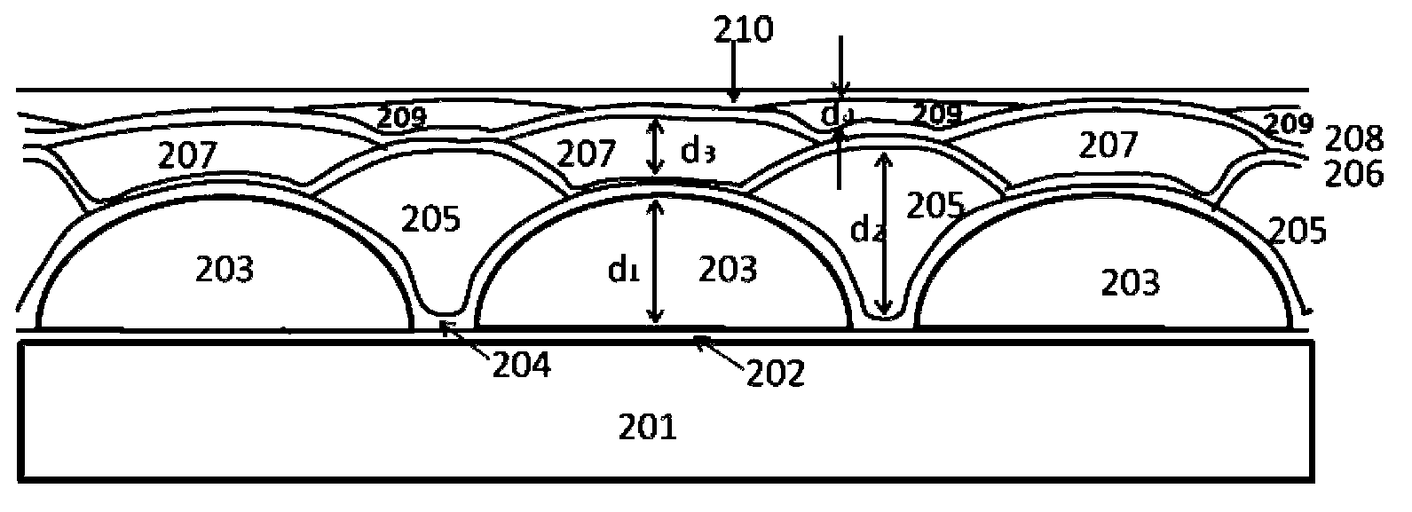
[0042] as attached Figure 2-3 As shown, a flexible substrate provided in this embodiment includes a PI substrate 201, a first barrier layer 202, a first planarization layer 203, a second barrier layer 204, a second The planarization layer 205 , the third barrier layer 206 , the third planarization layer 207 , the fourth barrier layer 208 , the fourth planarization layer 209 , and the fifth barrier layer 210 .

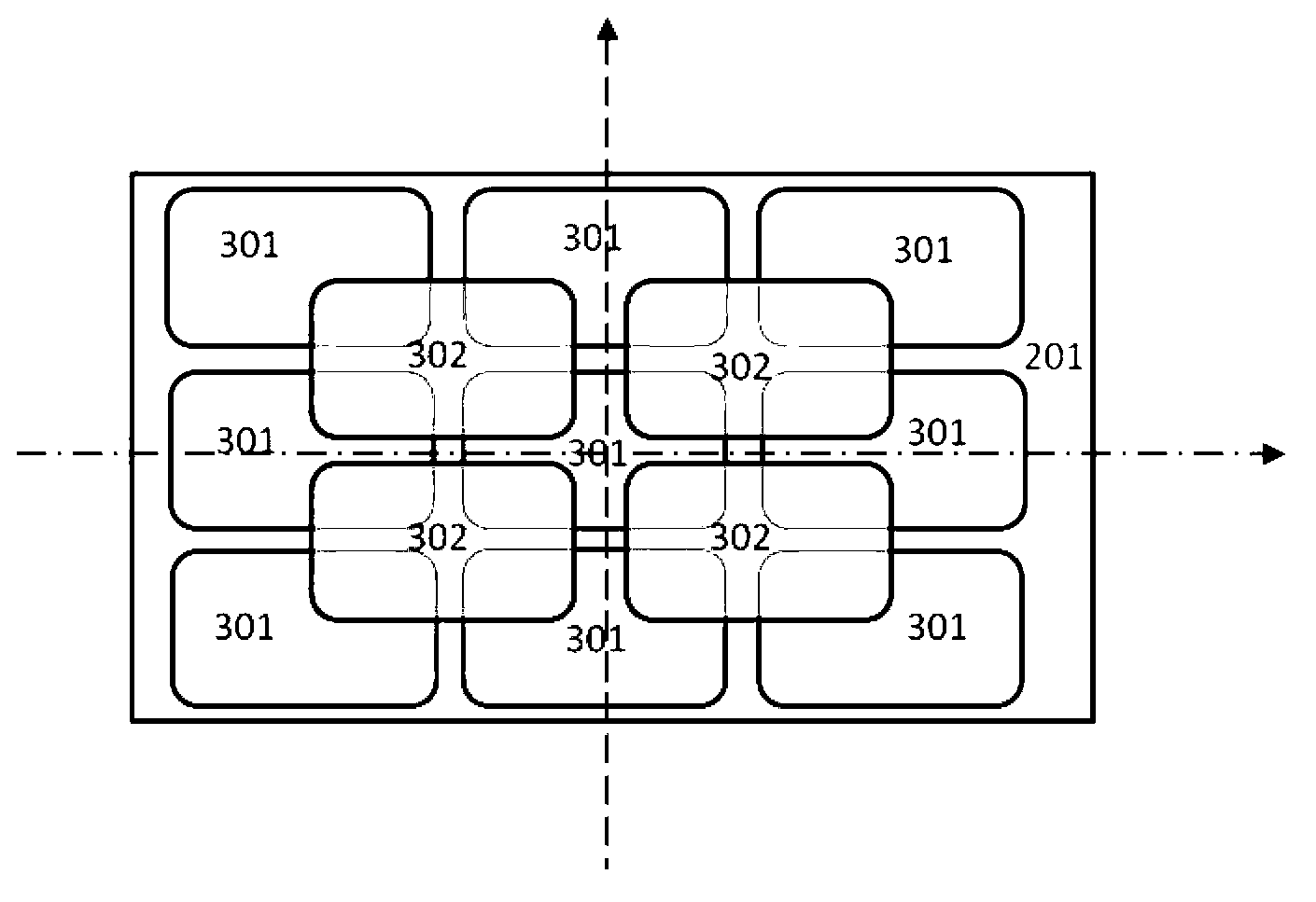
[0043] The first planarization layer 203, the second planarization layer 205, the third planarization layer 207, and the fourth planarization layer 209 are all composed of planarization units separated from each other and arranged periodically in the first direction and the second direction , the first direction and the second direction are as image 3 As shown in the direction of the middle arrow, the included angle is 90°. The patterns of the planarization units are the same, and the projections on the PI substrate 201 are all rectangles of the same size, the length ...

Embodiment 2

[0052] A flexible substrate structure provided in this embodiment is as figure 2 As shown, the preparation method is the same as in Example 1, the only difference is that the patterns of the planarization units in the first planarization layer 203, the second planarization layer 205, the third planarization layer 207, and the fourth planarization layer 209 Different from Example 1, such as Figure 4 As shown, the planarization units in the first planarization layer 203 and the third layer 207 are circles with equal radii, and the projections on the PI substrate 201 coincide, and the radius of the circles is 800 μm. The thickness of the first planarization layer is 2 μm, the thickness of the third planarization layer is 0.5 μm, and the distance between adjacent circles in the first direction and the second direction is equal, both are 200 μm; the second planarization layer 205 and The planarization unit in the fourth planarization layer 209 is a circle with a radius of 500 μm...

Embodiment 3

[0054] A flexible substrate structure provided in this embodiment is as figure 2 As shown, the preparation method is the same as that in Example 2, the only difference is that the arrangement of the planarization units in the first planarization layer 203, the second planarization layer 205, the third planarization layer 207, and the fourth planarization layer 209 The cloth method is different from Examples 1 and 2. In Embodiments 1 and 2, the planarization layer units are periodically arranged in the first direction and the second direction, and the angle between the two directions is 90°; and in this embodiment, as Figure 5 As shown, the planarization units are periodically arranged in the first direction and the second direction, and the angle between the two directions is 60°.

[0055] The planarization units in the first planarization layer 203 and the third layer 207 are circles with equal radii, the projections of 203 and 207 on the PI substrate 201 coincide, and the...


PUM


Abstract

The invention provides a flexible substrate. The flexible substrate comprises a polymer substrate and a plurality of barrier layers arranged on the polymer substrate. A planarization layer is arranged between adjacent barrier layer, each planarization layer comprises a plurality of planarization units which separate from one another in first and second directions, an included angle between the first direction and the second direction is 0 DEG-180 DEG, projections of the planarization units in the planarization layers on the substrate cover a gap between the projections of the planarization units on adjacent planarization layers, and projection areas partially overlap. Therefore, adjacent planarization layers can mutually cover position of the gap between the planarization units to stop transverse penetration of water and oxygen, the flexible substrate can be trimmed by optional size in a size range larger than the planarization units, large-scale production of the flexible substrate can be achieved, process step is simplified, and production cost is reduced. Thickness of odd layers and even layers in the planarization layers is decreased progressively in a direction far away from the substrate sequentially, and accordingly low roughness of the top surface of the flexible substrate is guaranteed and the flexible substrate is suitable for manufacturing of organic photoelectric devices.

Description

technical field [0001] The invention relates to the field of organic optoelectronics, in particular to a flexible substrate with water and oxygen barrier function for manufacturing organic optoelectronic devices such as OLED, OPV and OTFT. Background technique [0002] Organic electroluminescent diodes (English full name is Organic Light-Emitting Diodes, referred to as OLED), organic solar cells (English full name is Organic Photovoltaic, referred to as OPV), organic thin film field effect transistor (English full name is Organic Thin Film Transistor, referred to as The most attractive thing about organic optoelectronic devices such as OTFT) and organic optical pump lasers (English full name is Organic Semiconductor Lasers, referred to as OSL) is that they can be flexible. Specifically, organic optoelectronic devices are fabricated on flexible polymer substrates. , such as polyethylene (PE), polypropylene (PP), polystyrene (PS), polyavanether (PES), polyethylene terephthalat...

Claims


Application Information

Patent Timeline
Patent Type & Authority Applications(China)
IPC IPC(8): H01L51/00
CPCY02E10/549B32B27/14B32B3/10B32B2264/102B32B2307/7244B32B2307/7265B32B2457/00Y10T428/24521Y02P70/50H10K77/111H10K71/851H10K2102/311H10K50/8445H10K85/10H10K85/111
Inventor 朱少鹏邱勇陈红平山秀雄黄秀颀
Owner KUNSHAN NEW FLAT PANEL DISPLAY TECH CENT
Why Eureka
Try Eureka