
copper bonding wire

A bonding wire, copper alloy technology, applied in electrical components, circuits, electrical solid devices, etc., can solve the problem of high cost

Active Publication Date: 2015-09-23
HITACHI METALS LTD
View PDF13 Cites 0 Cited by
  • Summary
  • Abstract
  • Description
  • Claims
  • Application Information

AI Technical Summary

Problems solved by technology

[0003] Au wire has excellent electrical conductivity, corrosion resistance, and softness, but on the other hand, the cost is very high

Method used


Image

  • copper bonding wire
  • copper bonding wire
  • copper bonding wire

Examples


Embodiment 1

[0102] [Manufacture of soft low-concentration copper alloy material (2.6mm diameter)]

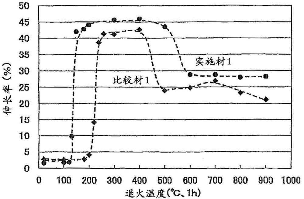
[0103] As a test material, a φ8 mm copper wire (wire rod, processing degree 99.3%) having an oxygen concentration of 7 mass ppm to 8 mass ppm, a sulfur concentration of 5 mass ppm, and a titanium concentration of 13 mass ppm was produced. The φ8mm copper wire was produced by performing hot rolling processing by the SCR continuous casting and rolling method (South Continuous Rod System). Regarding Ti, molten copper melted in a shaft furnace is made to flow in a tank under a reducing gas atmosphere, the molten copper flowing in the tank is introduced into a casting pot in the same reducing gas atmosphere, and Ti is added to the casting pot Afterwards, it is passed through a nozzle, and an ingot rod is made by using the mold formed between the casting wheel and the endless belt. This ingot rod was subjected to hot rolling processing to produce a φ8 mm copper wire. Next, cold wire drawing was...

Embodiment 2

[0124] [铜接合线]

[0125] The procedure was the same as in Example 1 of the above-mentioned soft low-concentration copper alloy material up to the production of a φ2.6 mm-sized copper wire. The above-mentioned copper wire was wire-drawn to φ0.9 mm, and once annealed in an electric annealing furnace, it was drawn to φ0.05 mm. Next, moving annealing was performed at 400° C. to 600° C. for 0.8 to 4.8 seconds in a tubular furnace to obtain a material for Example material 2 . As a comparison, 4N copper (99.99% or more, OFC (oxygen-free copper)) with a diameter of 0.05mm was also produced under the same processing and heat treatment conditions, and it was made into the material of comparative material 2. The mechanical properties (tensile strength, elongation, hardness), grain size of these materials were determined.

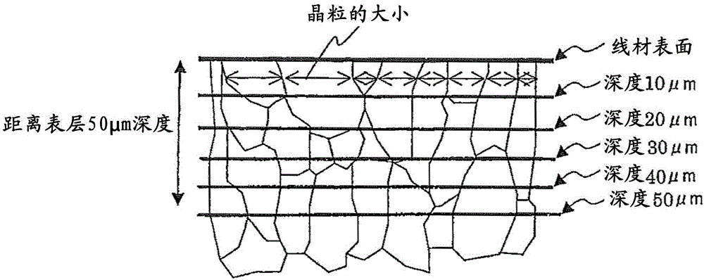
[0126] The average crystal grain size in the surface layer measures the crystal grain size in the range of length 0.025 mm from the surface in the radial cross-section...

Embodiment 3

[0155] (Regarding the crystal structure of a copper bonding wire with a diameter of 0.26mm at an annealing temperature of 600°C)

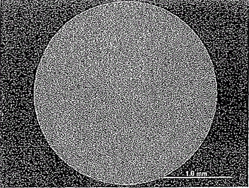
[0156] Figure 11 A cross-sectional photograph showing the radial cross-sectional structure of a sample of Example Material 3, which has the same composition as Example Material 1 and was annealed at an annealing temperature of 600°C for 1 hour with respect to a wire rod with a diameter of 0.26 mm, Figure 12 It is a diagram showing a cross-sectional photograph of a radial cross-sectional structure of Comparative Material 3.

[0157] Such as Figure 11 with Figure 12 As shown, in the crystal structure of Comparative Material 3, crystal grains of equal size are uniformly arranged as a whole from the surface portion to the central portion. On the other hand, in the crystal structure of Example Material 3, the crystal grain size is sparse as a whole. In particular, the crystal grain size in the layer formed thinly near the surface in the cross-sec...


PUM

PropertyMeasurementUnit
particle sizeaaaaaaaaaa
tensile strengthaaaaaaaaaa
Vickers hardnessaaaaaaaaaa

Abstract

PROBLEM TO BE SOLVED: To provide a copper bonding wire having high tensile strength and elongation and small rigidity. SOLUTION: The copper bonding wire consists of a soft thin copper alloy material which includes an additive element selected from a group consisting of Ti, Mg, Zr, Nb, Ca, V, Ni, Mn and Cr and whose remainder is copper and inevitable impurity. In a crystalline structure, an average crystal particle size to depth which is 20% of a wire diameter from at least a surface to an inner part is 20 μm or below.

Description

technical field [0001] The present invention relates to new copper bonding wires having high tensile strength, elongation, and low hardness. Background technique [0002] Conventionally, Au wires or Al alloy wires have been used as bonding wires for connecting electrodes of semiconductor elements to external leads. In particular, in resin mold type semiconductor elements, Au wires with a diameter of about 0.025 mm are used from the viewpoint of connection reliability. In addition, in recent years, Al wires with a diameter of about 0.3 mm have been used as bonding wires for power modules for automobiles. [0003] Au wire has excellent electrical conductivity, corrosion resistance, and softness, but on the other hand, the cost is very high. Therefore, bonding wires using copper (Cu) as a raw material have been proposed. [0004] In Patent Document 1, it is known that a fine copper wire for bonding that is highly purified to a purity of 99.999% by mass or higher by electroly...

Claims


Application Information

Patent Timeline
Patent Type & Authority Patents(China)
IPC IPC(8): C22C9/00H01L23/49
CPCH01L2224/45644H01L24/05H01L2224/05624H01L2224/45147H01L2224/45124H01L24/43H01L2224/45618H01L2224/45015H01L24/45H01L2224/45014H01L2224/43848H01L2224/45639H01L2924/10253H01L2924/01047H01L2924/01028H01L2924/00014H01L2224/48724H01L2224/45565H01L2924/01029H01L2224/45664H01L2224/48824H01L2224/45669H01L2924/01006H01L2224/45655H01L2224/43H01L2224/45H01L2224/45144H01L2924/00011H01L2924/01022H01L2924/01012H01L2924/0104H01L2924/01041H01L2924/0102H01L2924/01023H01L2924/01025H01L2924/01024H01L2924/00H01L2924/013H01L2224/48H01L2924/01205H01L2924/20751H01L2924/20752H01L2924/00015H01L2924/2076H01L2924/20108H01L2924/20109H01L2924/2011H01L2924/20111H01L2924/00012H01L2924/01033H01L2924/01008H01L2924/01016
Inventor 佐川英之青山正义黑田洋光鹫见亨藤户启辅冈田良平
Owner HITACHI METALS LTD
Learn More