Solution method electrolyte thin film transistor and preparation method thereof

A technology for electrolyte thin films and transistors, which is applied in the manufacture of transistors, electrical solid devices, semiconductor/solid devices, etc., can solve the problems of restricting the industrial development of thin film transistors, increasing device processing costs and energy consumption, and complicating the processing process. The effect of reducing processing cost, reducing working voltage and simplifying processing technology

Inactive Publication Date: 2013-04-17
SHANGHAI JIAO TONG UNIV
View PDF3 Cites 15 Cited by
  • Summary
  • Abstract
  • Description
  • Claims
  • Application Information

AI Technical Summary

Problems solved by technology

However, most of the current processes require two or more evaporation processes to process the gate and source drain separately, which undoubtedly complicates the process, increases device processing costs and energy consumption, and limits the process to a certain extent. Further Development of Thin Film Transistor Industrialization

Method used


Image

  • Solution method electrolyte thin film transistor and preparation method thereof
  • Solution method electrolyte thin film transistor and preparation method thereof
  • Solution method electrolyte thin film transistor and preparation method thereof

Examples


preparation example Construction

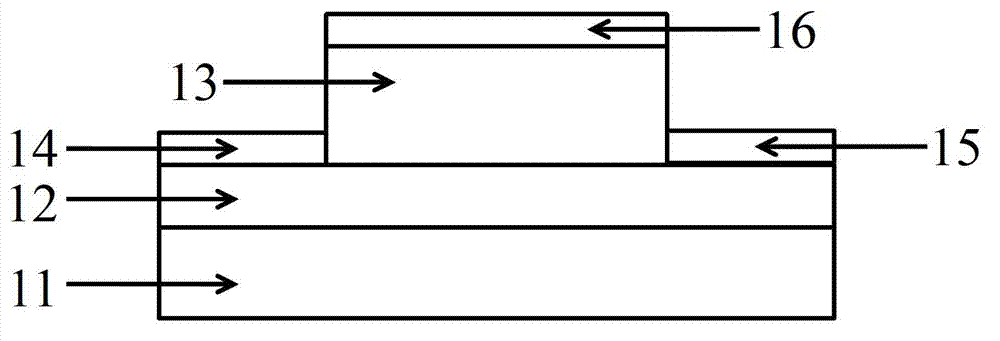
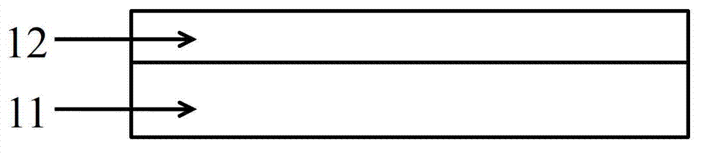
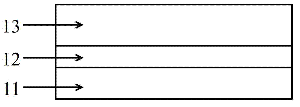
[0033] see Figure 2A — Figure 2D , the specific steps of the preparation method of the solution method bipolar thin film transistor are as follows:

[0034] 1) Preparing the semiconductor layer 12 on the insulating substrate 11, the preparation method used is a solution method such as spin coating, inkjet printing, screen printing or pulling method;

[0035] 2) Preparing the electrolyte insulating layer 13 on the semiconductor layer 12, the preparation method used is solution spin coating, spray coating or scraping coating of the electrolyte insulating layer solution;

[0036] 3) Perform patterning treatment on the electrolyte insulating layer 13, the treatment method used is to use a mask with a certain pattern for photocrosslinking, and then use a certain solvent for elution treatment, so that the electrolyte insulation layer 13 after the elution treatment Only covering part of the upper surface of the semiconductor layer 12, exposing the semiconductor layer 12 on both s...

Embodiment 1

[0040] 1) Prepare a semiconductor layer 12 on a glass insulating substrate 11, the material of the semiconductor layer 12 is an electronically conductive inorganic oxide semiconductor processed by a solution method, and the preparation method used is a solution method spin coating.

[0041] 2) Prepare an electrolyte insulating layer 13 on the semiconductor layer 12, the electrolyte insulating layer 13 is a polymer electrolyte insulating layer material PVA+KF processed by a solution method, and the preparation method used is spin coating an electrolyte insulating layer solution by a solution method.

[0042] 3) Perform patterning treatment on the electrolyte insulating layer 13, the treatment method used is to use a mask with a certain pattern for photocrosslinking, and then use a certain solvent for elution treatment, so that the electrolyte insulation layer 13 after the elution treatment Only part of the upper surface of the semiconductor layer 12 is covered, and the semicondu...

Embodiment 2

[0045] 1) Prepare the semiconductor layer 12 on the insulating substrate 11 of the plastic film, the material of the semiconductor layer 12 is a small molecule semiconductor with hole conduction processed by solution method, and the preparation method used is inkjet printing by solution method.

[0046]2) Prepare an electrolyte insulating layer 13 on the semiconductor layer 12, the electrolyte insulating layer 13 is a polymer electrolyte insulating layer material PS-PMMA-PS+[EMIM][TFSI] processed by a solution method, and the preparation method used is spray coating by a solution method Electrolyte insulating layer solution.

[0047] 3) Perform patterning treatment on the electrolyte insulating layer 13, the treatment method used is to use a mask with a certain pattern for photocrosslinking, and then use a certain solvent for elution treatment, so that the electrolyte insulation layer 13 after the elution treatment Only part of the upper surface of the semiconductor layer 12 i...


PUM


Abstract

The invention discloses a solution method electrolyte thin film transistor and a preparation method thereof. The electrolyte thin film transistor is in a top gate top contact structure and comprises an insulating substrate, a semiconductor layer, an electrolyte insulating layer, a source electrode and a gate electrode, wherein the insulating substrate is positioned on the bottom layer of the electrolyte thin film transistor; the semiconductor layer is positioned above the insulating substrate; the electrolyte insulating layer is covered above parts of upper surface of the semiconductor layer; the source electrode and the drain electrode are respectively arranged on the semiconductor layer on two sides of the electrolyte insulating layer and are separated by the electrolyte insulating layer; and the gate electrode is arranged on the electrolyte insulating layer. The preparation method comprises the following steps of: carrying out patterning photo-crosslinking treatment; processing parts of electrolyte insulating layer by solvent; carrying out single-time vacuum vapor deposition; and simultaneously and respectively forming a gate electrode, a source electrode and a drain electrode by the surface height difference. According to the invention, low on-state voltage and big working current are realized, the processing technology is simplified, the cost is lowered, and the invention is suitable for the low-cost flexible electronic technology.

Description

technical field [0001] The invention relates to a field-effect transistor, more specifically, to a solution-process electrolyte thin film transistor and a preparation method thereof, belonging to the technical field of flexible electronics. Background technique [0002] Solution thin film transistors have attracted widespread attention due to their advantages of low cost, low temperature preparation, easy flexibility, and large area integration. practical application. With people's ever-increasing requirements for low cost and portability of electronic products, the development of solution-based thin film transistors is bound to receive greater promotion and attention. [0003] Using the polymer electrolyte material as the insulating layer of the organic thin film transistor can increase the drain output current and reduce the operating voltage of the transistor on the basis of increasing the thickness of the insulating layer. This kind of transistor with low operating vol...

Claims


Application Information

Patent Timeline
Patent Type & Authority Applications(China)
IPC IPC(8): H01L51/10H01L51/30H01L51/40H01L29/786H01L29/49H01L21/336
Inventor 邵宪一冯林润唐伟李思莹郭小军
Owner SHANGHAI JIAO TONG UNIV
Why Eureka
Try Eureka