High-sensitivity solid-state color image sensor

A color image, high-sensitivity technology, applied in the direction of radiation control devices, etc., can solve the problems of reducing detection accuracy, affecting detection sensitivity and dynamic range, and achieve the effect of mature technology, improved sensitivity and dynamic range, and easy realization

Active Publication Date: 2013-04-24
NANJING UNIV OF POSTS & TELECOMM INST AT NANJING CO LTD
View PDF5 Cites 6 Cited by
  • Summary
  • Abstract
  • Description
  • Claims
  • Application Information

AI Technical Summary

Problems solved by technology

As the size of the device decreases, the area of ​​the conversion region decreases, so that the photoelectrons generated and collected also decrease, which affects the sensitivity and dynamic range of detection.
In addition, the channel region of the device is used as a photoelectron generation and collection region. When the energy of the incident photons is very large, such as in the ultraviolet light band, the charge on the device storage layer will gain enough energy to escape from the memory, or the device substrate or gate The electrons will directly enter the storage layer, changing the charge amount and charge distribution in the storage layer, thereby reducing the detection accuracy

Method used


Image

  • High-sensitivity solid-state color image sensor
  • High-sensitivity solid-state color image sensor
  • High-sensitivity solid-state color image sensor

Examples


Embodiment Construction

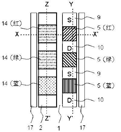
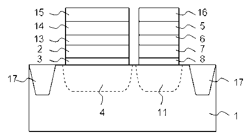
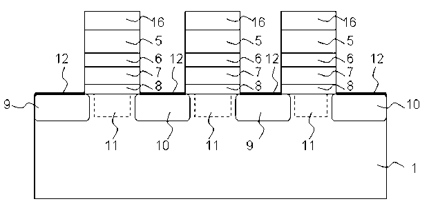
[0021] (1) Color image sensor structure

[0022] The top and cross-sectional schematic diagrams of the color image sensor pixel unit are shown in Figure 1 ~ Figure 4 shown. Each red, green, and blue pixel sub-unit is composed of a MOS capacitor and a MOSFET structure storage tube respectively. The P-type silicon substrate material 1 Accumulation gate with large area above 2 , an insulating dielectric layer is provided between the accumulation gate and the P-type silicon substrate 3 , the accumulation gate-insulating dielectric layer-P-type semiconductor silicon substrate forms a MOS capacitor, and the silicon substrate under the accumulation gate is the photoelectric conversion region 4 . Next to the accumulation gate is a control gate perpendicular to the accumulation gate 5 . A blocking insulating dielectric layer is sequentially arranged directly below the control grid 6 , Optoelectronic storage layer 7 , tunnel oxide 8 and P-type semiconductor silicon substrate ...


PUM


Abstract

The invention discloses a high-sensitivity solid-state color image sensor. Particularly, a large-area MOS (Metal Oxide Semiconductor) capacitor is used as a photoelectric conversion region, the generated and collected photoelectrons are transferred to a channel region arranged below the grid electrode of an adjacent small-sized MOSFET (Metal-Oxide-Semiconductor Field Effect Transistor) storage, furthermore, the transferred photoelectrons are injected into a storage layer of the storage to enable the threshold voltage of the storage to change, and finally, the intensity of the detected light is determined through reading the drain current of the storage. Pixel units of the color image sensor are as follows: each pixel unit of the color image sensor is composed of three pixel subunits which have the same structures and are respectively red, green and blue, and each of the red, green and blue pixel units is respectively composed of one MOS capacitor and one MOSFET structural storage tube. A manufacturing process of the color image sensor is completely compatible with a CMOS (Complementary Metal-Oxide-Semiconductor) process; and the color image sensor is matured in process, low in cost and easy to achieve.

Description

technical field [0001] The invention relates to a solid-state image sensing device, especially a high-sensitivity, low-cost color solid-state image sensing device based on CMOS technology, which can be used as an imaging device in products such as video cameras, digital cameras, palmtop computers, mobile phones, and PDAs. [0002] Background technique [0003] There are two main types of solid-state image sensing devices widely used now: charge-coupled device (CCD) and CMOS active pixel sensor APS. Although CCD sensors are superior to CMOS sensors in terms of sensitivity, resolution, and noise control, they have the disadvantages of complex process, high cost, large device size, small integration, slow imaging speed, high power consumption, and need for multiple power sources; and CMOS sensors have the advantages of low cost, low power consumption, and high integration, but they also have problems such as low sensitivity, high noise, and small dynamic range. It can be seen...

Claims


Application Information

Patent Timeline
Patent Type & Authority Applications(China)
IPC IPC(8): H01L27/146
Inventor 徐跃赵菲菲岳恒
Owner NANJING UNIV OF POSTS & TELECOMM INST AT NANJING CO LTD
Why Eureka
Try Eureka