Germanium silicon heterojunction bipolar transistor and manufacturing method thereof

A technology of heterojunction bipolar and manufacturing method, which is applied in the manufacture of germanium-silicon heterojunction bipolar transistors, and in the field of germanium-silicon heterojunction bipolar transistors, which can solve the problem of the number of photolithography layers and the collector connection layer of the HBT process. Problems such as high resistance and high epitaxy cost in the collector area can achieve the effect of high diffusion rate, improved N-type impurity distribution, and uniform impurity concentration distribution

Active Publication Date: 2013-04-24
SHANGHAI HUAHONG GRACE SEMICON MFG CORP
View PDF3 Cites 2 Cited by
  • Summary
  • Abstract
  • Description
  • Claims
  • Application Information

AI Technical Summary

Problems solved by technology

The technology of this device is mature and reliable, but the main disadvantages are: 1. The epitaxy cost of the collector area is high; 2. The formation of collector pick-up depends on high-dose and high-energy ion implantation to lead out the buried layer of the collector area. The device area is large; 3. The deep trench isolation process is complicated and the cost is high; 4. The number of photolithography layers in the HBT process is large
[0005] There are also some problems in the existing improved process. For example, the junction formed by low-energy N-type impurity implantation is relatively shallow, resulting in a thinner N-type buried layer (Pseudo Buried Layer), and the resistance of the collector connection layer (Rc) is relatively low. High, and the contact resistance is too large, making it difficult to increase the cut-off frequency (Ft)

Method used


Image

  • Germanium silicon heterojunction bipolar transistor and manufacturing method thereof
  • Germanium silicon heterojunction bipolar transistor and manufacturing method thereof
  • Germanium silicon heterojunction bipolar transistor and manufacturing method thereof

Examples


Embodiment Construction

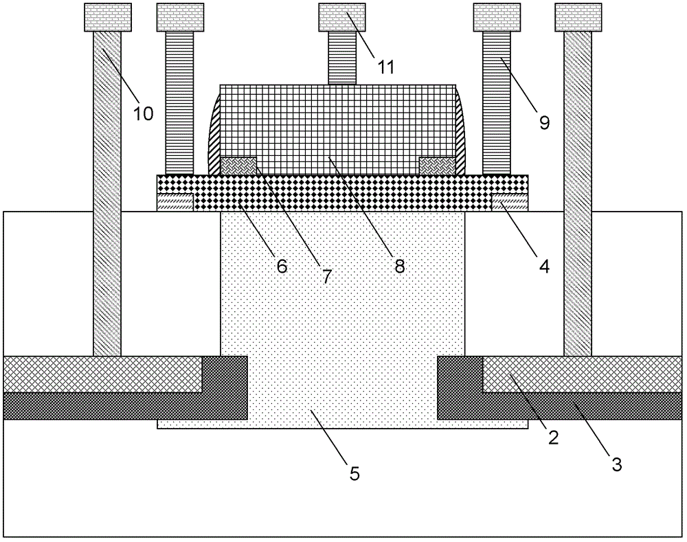
[0030] Such as figure 1 Shown is a schematic diagram of the structure of a silicon germanium heterojunction bipolar transistor device according to an embodiment of the present invention. The silicon germanium heterojunction bipolar transistor of the embodiment of the present invention is formed on a silicon substrate, and the active region is isolated by shallow trench field oxygen. The silicon germanium heterojunction bipolar transistor includes:

[0031] The collector region 5 is composed of an N-type ion implantation region formed in the active region. The depth of the collector region 5 is greater than the depth of the oxygen bottom of the shallow trench field, and the collector region 5 extends laterally Enter the bottom of the shallow groove field oxygen on both sides of the active region. A groove is formed at the bottom of the shallow groove field oxygen on the peripheral side of the active region, the width of the groove is less than or equal to the width of the bottom o...


PUM

PropertyMeasurementUnit
thicknessaaaaaaaaaa

Abstract

The invention discloses a germanium silicon heterojunction bipolar transistor. A groove is formed in the bottom of shallow groove field oxygen in the circumstance of an active region, polycrystalline silicon is filled in the groove, a polycrystalline silicon burying layer is formed by the polycrystalline silicon filled in the groove, N type impurities are mixed with the polycrystalline silicon burying layer, the N type impurities further spread to a silicon substrate in the circumstance of the polycrystalline silicon burying layer to form a first N type impurities region, a collector connecting layer is formed by the polycrystalline silicon burying layer and the first N type impurities region, the collector connecting layer is contacted with a collector region at the bottom of the shallow groove field oxygen, and a deep hole contact area is formed in the shallow groove field oxygen on the top of the pseudo buried layer and leads a collector out. The invention further discloses a manufacturing method of the germanium silicon heterojunction bipolar transistor. According to the germanium silicon heterojunction bipolar transistor and the manufacturing method thereof, the thickness of the collector connecting layer can be increased to enable the distribution of impurities to be even, the resistance and the contact resistance of the collector connecting layer can be reduced and the value of the resistance and the contact resistance are enabled to be even, and thus the cut-off frequency of the germanium silicon HBT (SiGe HBT) can be improved.

Description

Technical field [0001] The invention relates to the field of semiconductor integrated circuit manufacturing, in particular to a silicon germanium heterojunction bipolar transistor; the invention also relates to a manufacturing method of a silicon germanium heterojunction bipolar transistor. Background technique [0002] In RF applications, higher and higher device characteristic frequencies are required. Although RFCMOS can achieve higher frequencies in advanced process technology, it is still difficult to fully meet the RF requirements. For example, it is difficult to achieve characteristic frequencies above 40GHz and advanced technology. The research and development cost of compound semiconductors is also very high; compound semiconductors can realize very high characteristic frequency devices, but due to the high material cost, small size, and most compound semiconductors are toxic, their applications are limited. Silicon germanium (SiGe) heterojunction bipolar transistor (HBT...

Claims


Application Information

Patent Timeline
Patent Type & Authority Applications(China)
IPC IPC(8): H01L29/737H01L29/08H01L21/331H01L21/225
Inventor 陈帆陈雄斌薛凯周克然潘嘉李昊
Owner SHANGHAI HUAHONG GRACE SEMICON MFG CORP
Why Eureka
Try Eureka