Laser annealing device and laser annealing method

A laser annealing and laser technology, applied in laser welding equipment, electrical components, circuits, etc., can solve problems such as low beam quality

Active Publication Date: 2013-05-01
JSW阿克迪纳系统有限公司
View PDF17 Cites 1 Cited by
  • Summary
  • Abstract
  • Description
  • Claims
  • Application Information

AI Technical Summary

Problems solved by technology

In excimer lasers, the beam quality is low, so ...

Method used


Image

  • Laser annealing device and laser annealing method
  • Laser annealing device and laser annealing method
  • Laser annealing device and laser annealing method

Examples


Embodiment 1

[0095] Next, examples of the present invention will be described in comparison with comparative examples.

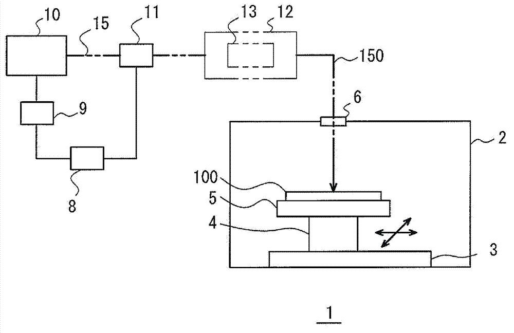
[0096] Utilize the laser annealing apparatus of above-mentioned embodiment ( figure 1 ), an experiment of irradiating pulsed laser light at 50 nm to an amorphous silicon thin film formed on the surface of a glass substrate by a common method was carried out.

[0097] In this experiment, the pulsed laser was shaped by the light transmission unit so that the processed surface became a rectangle, and the energy density on the irradiated surface was set to be 8-400mJ / cm 2 , The pulse width is in the range of 20-600ns to irradiate the amorphous silicon on the substrate. In addition, the absorption coefficient of the amorphous silicon film is defined as absorption coefficient=4πk / wavelength.

[0098] (k: Attenuation coefficient refers to non-patent literature: D.E.Aspnes and J.B.Theeten, J.Electrochem.Soc.127,1359(1980))

[0099] Amorphous silicon is heated by irradiation ...

Embodiment 2

[0105] If a XeCl excimer laser is used for the laser oscillator, set the effective power density to 2.7×10 12 When irradiated with pulsed laser light, as shown in photo 2, uniform crystals without spots are formed.

Embodiment 3

[0107] If a YAG third harmonic solid-state laser is used for the laser oscillator, set the effective power density to 1.8×10 12 When irradiated with pulsed laser light, as shown in photo 3, uniform crystals without spots are formed.


PUM


Abstract

The present invention enables uniform crystallization of a semiconductor film by means of laser annealing. The present invention comprises a pulse laser oscillating device for outputting a pulse laser beam, and an optical transmission means for transmitting the pulse laser beam outputted from the pulse laser oscillating device to irradiate onto the semiconductor film. Since the pulse laser beam, which has an effective power density on the irradiated surface of the semiconductor film calculated by the formula of effective power density (J / (sec.cm3)) = pulse energy density (J/cm2) / pulse width (sec) absorption coefficient of semiconductor film (cm-1), is irradiated onto the semiconductor film so as to be in a range of 3 1012 to 1.5 1012, the semiconductor film can be crystallized without inducing abnormal grain growth due to complete melting, and uniform crystals with little variation are obtained.

Description

technical field [0001] The present invention relates to a laser annealing device and a laser annealing method for performing laser annealing by irradiating pulsed laser light on a semiconductor film. Background technique [0002] In recent years, the keywords of liquid crystal displays are high resolution, high-speed drive frame rate, 3D, etc., and thin film transistors having the performance required to achieve the above-mentioned objects are required. In order to improve the performance of thin film transistors, it is necessary to crystallize the silicon semiconductor film by laser degradation. [0003] Conventionally, a laser annealing apparatus is an apparatus for crystallizing amorphous silicon (a-Si), and an annealing technology using an excimer laser is used. In the excimer laser, the quality of the beam is low, so the beam cannot be shrunk down to a small size. Therefore, it is used after combining the optical system and shaping the beam into a beam with a flat top...

Claims


Application Information

Patent Timeline
IPC IPC(8): H01L21/268H01L21/20
CPCH01L21/268B23K26/0676H01L21/02532B23K26/0608B23K26/0613H01L21/02686H01L21/20
Inventor 佐藤亮介草间秀晃富樫陵太郎井崎博大
Owner JSW阿克迪纳系统有限公司
Why Eureka
Try Eureka