InP single crystal wafer twin polishing method and device

A double-sided polishing, double-sided polishing machine technology, applied in the field of materials

Inactive Publication Date: 2015-07-01
CHINA ELECTRONICS TECH GRP NO 46 RES INST
View PDF4 Cites 0 Cited by
  • Summary
  • Abstract
  • Description
  • Claims
  • Application Information

AI Technical Summary

Problems solved by technology

However, the current double-sided polishing method of indium phosphide single crystal needs to be further improved

Method used


Image

  • InP single crystal wafer twin polishing method and device

Examples


Embodiment Construction

[0022] Preferred embodiments of the present invention will be specifically described below in conjunction with the accompanying drawings, wherein the accompanying drawings constitute a part of the application and are used together with the embodiments of the present invention to explain the principle of the present invention.

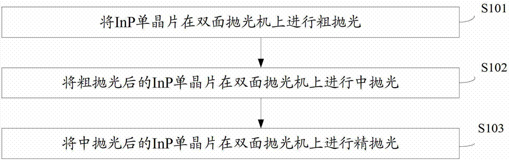
[0023] Embodiments of the present invention provide a double-sided polishing method for an InP single wafer, see figure 1 , the method includes:

[0024] S101, roughly polishing the InP single wafer on a double-sided polishing machine;

[0025] The rough polishing liquid in the embodiment of the present invention comprises alkaline colloidal silicon dioxide suspension, deionized water and sodium dichloroisocyanurate, and alkaline colloidal silicon dioxide suspension: deionized water: sodium dichloroisocyanurate The volume ratio is 1:10:(1.0~1.8), the pH value of the rough polishing liquid is 10-11, and the pressure of the rough polishing is (150~170) g...


PUM


Abstract

The invention discloses an InP single crystal wafer twin polishing method. The InP single crystal wafer twin polishing method comprises the steps that an InP single crystal wafer sequentially conducts rough polishing, moderate polishing and fine polishing on a twin polishing machine; rough polishing liquid comprises basoid silicon dioxide suspension liquid, deionized water and sodium dichloro cyanurate, volume ratio of the basoid silicon dioxide suspension liquid: the deionized: sodium dichloro cyanurate is 1:10:(1.0-1.8), and pondus hydrogenii (PH) value of the rough polishing liquid is 10-11; moderate polishing liquid comprises basoid silicon dioxide suspension liquid, deionized water and sodium hypochlorite, volume ratio of the basoid silicon dioxide suspension liquid: the deionized: the sodium hypochlorite is 1:15:(0.1-0.5), and PH value of the moderate polishing liquid is 8-9; and fine polishing liquid comprises basoid silicon dioxide suspension liquid and deionized water, volume ratio of the basoid silicon dioxide suspension liquid: the deionized is 1: ( 40-60), and PH value of the fine polishing liquid is 7-8. Surface quality of the InP single crystal wafer which is obtained after polishing by adopting of the method is consistent, and the InP single crystal wafer is crocodile-skin-free, scratching-free and mist-free.

Description

technical field [0001] The invention relates to the field of materials, in particular to a double-sided polishing method and device for an InP single wafer. Background technique [0002] Indium phosphide (InP) crystal is an important semiconductor material. Compared with gallium arsenide (GaAs) materials, it has the characteristics of high electronic limit drift speed, good radiation resistance, high thermal conductivity, and high breakdown electric field. Therefore, the operating frequency limit of InP devices is twice as high as that of GaAs devices, with greater output power and better noise characteristics, and the radiation resistance performance is superior to GaAs and silicon (Si) materials. Therefore, InP materials are the preferred substrate materials in the preparation of microwave, millimeter wave circuits and high-speed digital integrated circuits. [0003] With the successful use of InP single-wafer polished wafers in microwave and millimeter-wave devices, peop...

Claims


Application Information

Patent Timeline
Patent Type & Authority Patents(China)
IPC IPC(8): B24B37/08
Inventor 林健赵权杨洪星王云彪武永超刘春香张伟才吕菲佟丽英
Owner CHINA ELECTRONICS TECH GRP NO 46 RES INST
Why Eureka
Try Eureka