Stereo display electrode and manufacturing method thereof

A technology of three-dimensional display and display electrodes, which is applied in the manufacture of semiconductor/solid-state devices, circuits, electrical components, etc., can solve the problem of difficult control of photolithography process accuracy and production time, and the inability to effectively use flat panel display space, raw materials, environmental burden and energy. High energy consumption and other issues, to achieve the effect of improving visible light transmittance, increasing volume, and improving electrical performance

Active Publication Date: 2013-05-15
DALIAN LONGNING TECH
View PDF10 Cites 8 Cited by
  • Summary
  • Abstract
  • Description
  • Claims
  • Application Information

AI Technical Summary

Problems solved by technology

The disadvantage is that this kind of electrode can only increase the contact area of ​​the interface, and cannot effectively use the space of the flat panel display to produce a low-resistance display electrode.
[0008] Although these inventions can improve the derivation efficiency in other fields such as organic solar cells and organic light-emitting diodes, they cannot be applied to the lead parts that require extremely low resistance in display fields such as liquid crystal and electronic paper.
The main reason is that the resistance of the above-mentioned ITO display electrode is still very large when there is a slight c

Method used


Image

  • Stereo display electrode and manufacturing method thereof
  • Stereo display electrode and manufacturing method thereof
  • Stereo display electrode and manufacturing method thereof

Examples


Embodiment 1

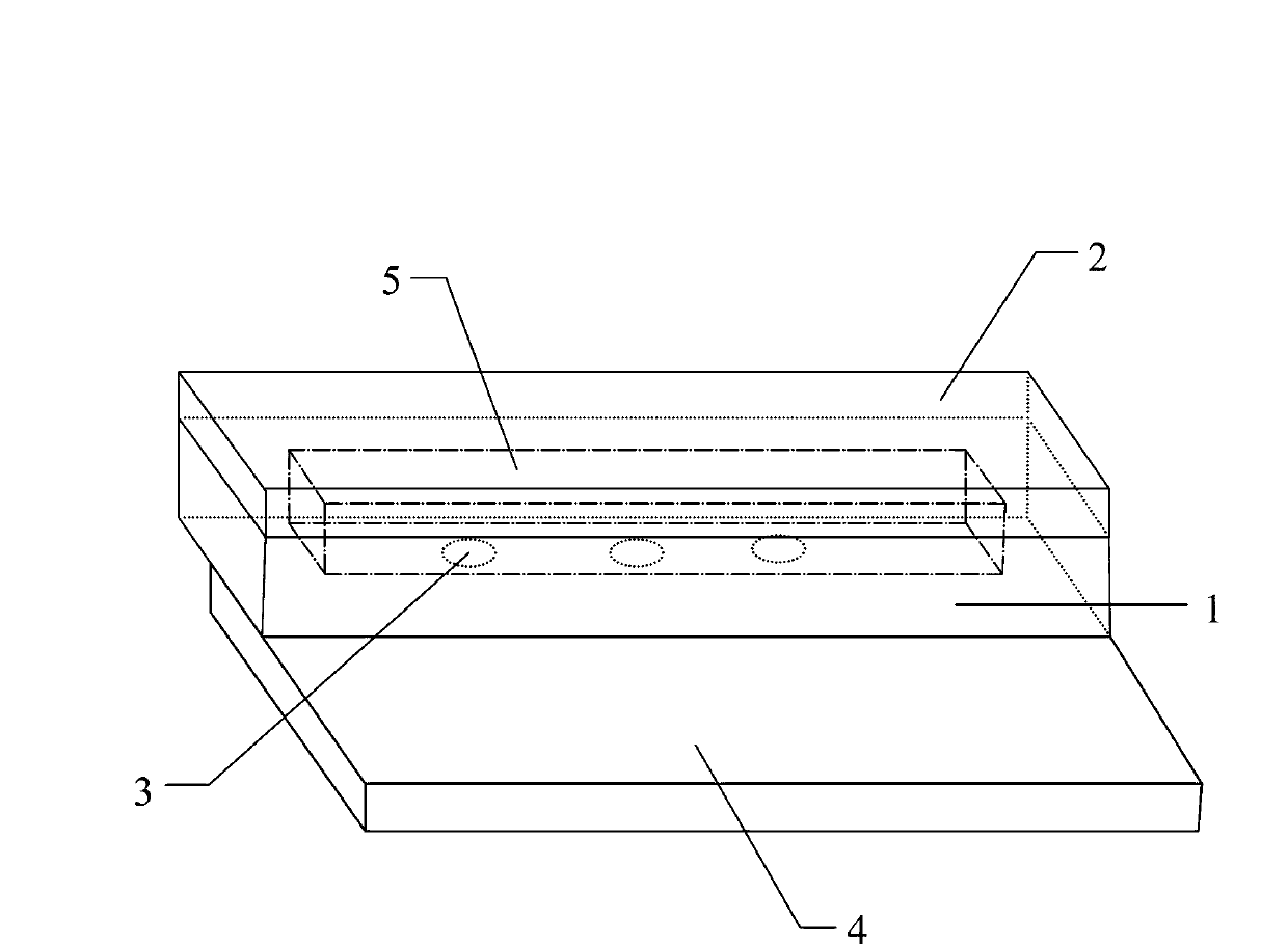
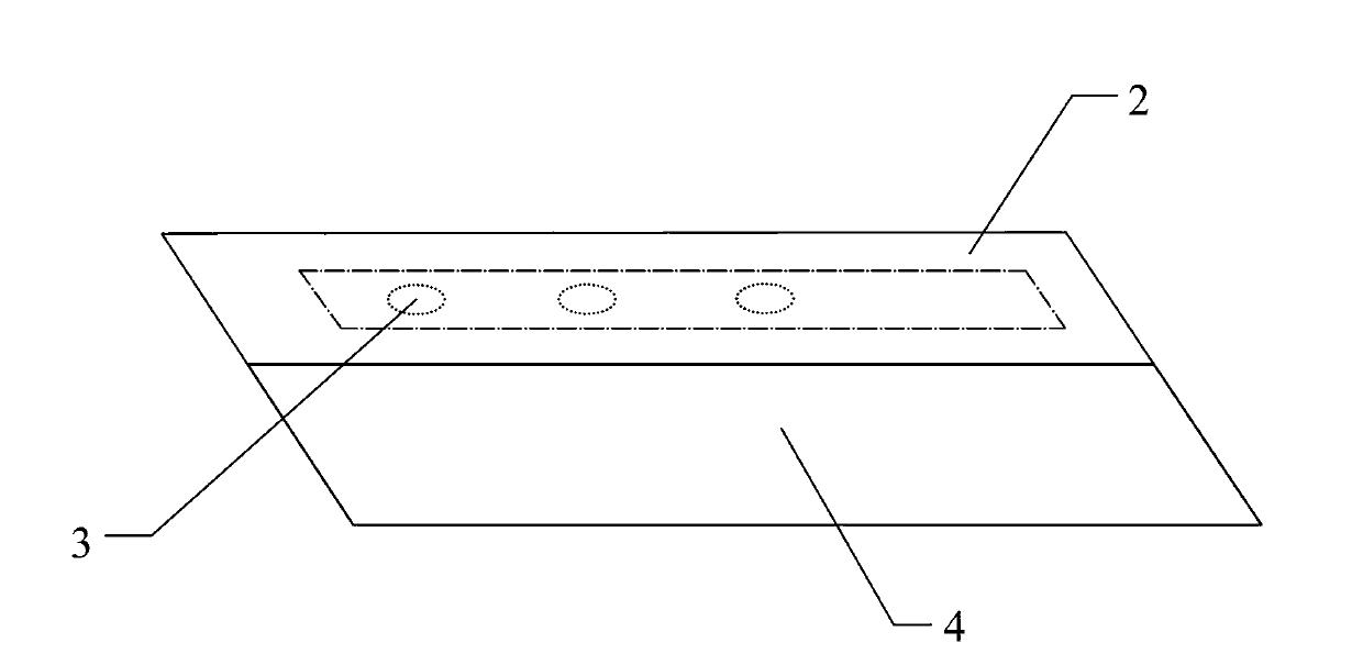
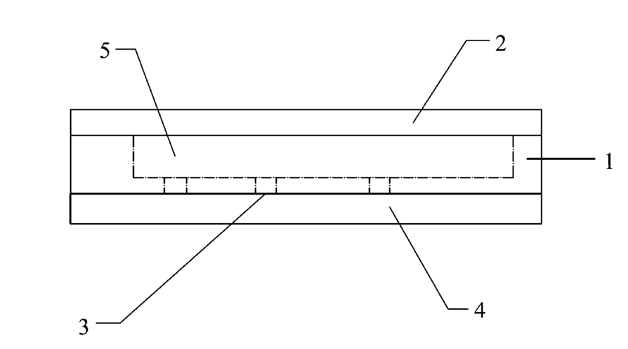
[0067] On the glass substrate, an inorganic three-dimensional display electrode is made, the insulating layer material is made of domestic Ruihong RZJ304 positive photoresist, and the sealing insulating layer is made of SW-B UV-cured epoxy resin. Inorganic conductive materials use silver nanoparticle ink (SEINTRONICS INK), which has good dispersion and conductivity necessary for the formation of inkjet printed circuits, and can form high-quality auxiliary three-dimensional electrodes due to the characteristics of non-agglomeration and less clogging . The transparent thin film display electrode uses ITO thin film.

[0068] The specific process is as follows:

[0069] The glass substrate is coated, and the ITO film thickness of the transparent film display electrode is 100 angstroms;

[0070] Scrub with cleaning solution, the water temperature is 40 ° C, and the concentration of the clear solution is 10%;

[0071] Rinse and dry with ultrapure water at 40°C;

[0072] UV light...

Embodiment 2

[0090] On the PET substrate, a three-dimensional display electrode mixed with inorganic and organic is made, the insulating layer material is made of domestic Ruihong RZJ304 positive photoresist, and the sealing insulating layer is made of SW-B UV-cured epoxy resin. The organic conductive material uses PEDOT:PSS solution to form high-quality auxiliary three-dimensional electrodes. The transparent thin film display electrode uses ITO thin film.

[0091] The specific process is as follows:

[0092] Coating at low temperature on the PET substrate, the ITO film thickness of the transparent film display electrode is 100 angstroms;

[0093] Rinse with cleaning solution, the water temperature is 40 ° C, and the concentration of the clear liquid is 10%;

[0094] Rinse and dry with ultrapure water at 40°C;

[0095] Slight exposure to ultraviolet light to remove organic matter;

[0096] Spin-coating photoresist, the thickness is controlled at 0.5μm;

[0097] Exposure, 10mj / cm 2 ; ...


PUM


Abstract

The invention discloses a stereo display electrode which comprises a transparent film display electrode and a stereo auxiliary electrode which is connected with the transparent film display electrode. The stereo display electrode is characterized in that the stereo auxiliary electrode comprises a formed insulating layer and a sealed insulating layer fixed at the upper end of the formed insulating layer, wherein a groove used for containing an electric conduction part is formed in the formed insulating layer, and the stereo auxiliary electrode is communicated with the transparent film display electrode through at least one communication hole which is formed at the lower end of the formed insulating layer. The invention further discloses a manufacturing method of the stereo display electrode. According to the stereo display electrode, the features of low resistance and high transparence are achieved, and low resistance, width minimization, even electric conductivity and flexibility and complete separation from display materials are achieved through the adjustment of thickness and material property of the stereo auxiliary electrode. The stereo display electrode can effectively reduce the resistance of an electrode, fully utilize redundancy space of an inner electrode of a display, and improve the resolution rate, refresh rate and contrast ratio of the display.

Description

technical field [0001] The invention relates to a three-dimensional display electrode and a manufacturing method thereof. The structure and manufacturing method of the three-dimensional display electrode can be applied to liquid crystal display devices, electronic paper displays and electroluminescent displays, especially active liquid crystal displays, passive cholesteric liquid crystal electronic paper, passive twisted nematic (TN , Twisted Nematic) and Super Twisted Nematic (STN, Super Twisted Nematic) displays, active electrochromic displays, electrophoretic electronic paper and organic light-emitting backplane electrodes. Background technique [0002] Since the application of flat-panel displays has been popularized, its display quality has been improved year by year, and its contrast, response speed and resolution are bringing people more and more visual enjoyment. These advancements and improvements are not only related to the innovation of display modes, but also ha...

Claims


Application Information

Patent Timeline
IPC IPC(8): H01L51/10H01L51/52H01L51/00G02F1/1343G02F1/167G02F1/155
Inventor 赵景罡
Owner DALIAN LONGNING TECH
Why Eureka
Try Eureka