Surface polishing method for GaN monocrystal substrate
A technology of polishing disk and polishing liquid, which is applied in the field of polishing, can solve problems such as V-shaped pits, large surface fluctuations, and crystal orientation selection, and achieve the effects of low pressure, low scratch density, and high polishing efficiency
- Summary
- Abstract
- Description
- Claims
- Application Information
AI Technical Summary
Problems solved by technology
Method used
Image

Examples
Embodiment 1
[0025] (1) Cut and orient the GaN crystal, and perform mechanical grinding on it. After grinding, the crystal plane of the GaN crystal is 0.6° from c to m plane, the thickness tolerance is less than 10 μm, and the root mean square of surface roughness is about 1-2.5nm .
[0026] (2) Wash the finely polished GaN with acetone, ethanol, and deionized water in sequence to remove oil stains on the back and surface, and then dry it with nitrogen gas for later use.
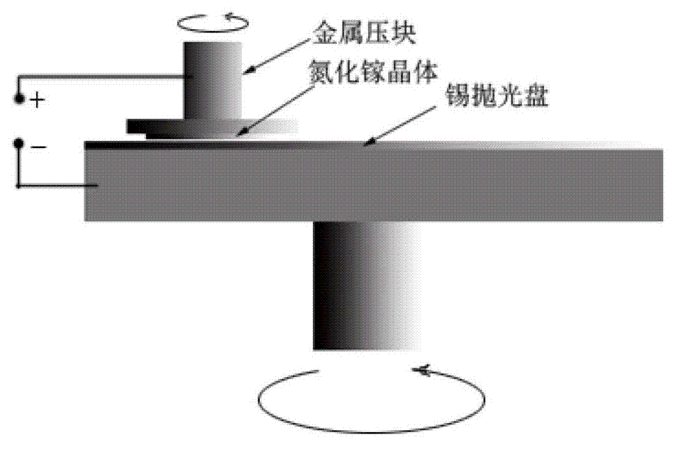
[0027] (3) Use thermoplastic conductive adhesive (paraffin: rosin: graphite = 1: 1.5: 0.2) to fix the cleaned GaN crystal on the metal polishing compact to ensure that the conductive adhesive coating on GaN is even and smooth.
[0028] (4) Use NaOH solution with a pH value of 9.5-11.5 as the polishing liquid.
[0029] (5) The GaN crystal is used as the anode to connect to the positive pole of the DC power supply, and the tin polishing disc is used as the cathode to connect to the negative pole of the DC power supply, an...
Embodiment 2
[0033] (1) Cut and orient the GaN crystal, and perform mechanical grinding on it. After grinding, the crystal plane of the GaN crystal is c-plane, the thickness tolerance is less than 20 μm, and the surface roughness root mean square is about 1-2.5 nm.
[0034] (2) Wash the finely polished GaN with acetone, ethanol, and deionized water in sequence to remove oil stains on the back and surface, and then dry it with nitrogen gas for later use.
[0035] (3) Use thermoplastic conductive adhesive (paraffin: rosin: graphite = 1: 1.5: 0.2) to fix the cleaned GaN crystal on the metal polishing compact to ensure that the conductive adhesive coating on GaN is even and smooth.
[0036] (4) Use a citric acid solution with a pH of 3.8-4.6 as the polishing fluid.
[0037] (5) The GaN crystal is used as the anode to connect to the positive pole of the DC power supply, and the tin polishing disc is used as the cathode to connect to the negative pole of the DC power supply. The output current ...
Embodiment 3
[0041] (1) Cut and orient the GaN crystal, and mechanically grind it. After grinding, the crystal plane of the GaN crystal is the c-plane, the thickness tolerance is less than 20 μm, and the root mean square of the surface roughness is about 1-2.5 nm.
[0042] (2) Wash the finely polished GaN with acetone, ethanol, and deionized water in sequence to remove oil stains on the back and surface, and then dry it with nitrogen gas for later use.
[0043] (3) Use thermoplastic conductive adhesive (paraffin: rosin: graphite = 1: 1.5: 0.2) to fix the cleaned GaN crystal on the metal polishing compact to ensure that the conductive adhesive coating on GaN is even and smooth.
[0044] (4) Use a 10wt% aqueous solution of silicon dioxide with a particle size of 50nm, adjust the pH to 9.5-11.5, and add a small amount of EDTA as a polishing solution.
[0045] (5) The GaN crystal is used as the anode to connect to the positive pole of the DC power supply, and the tin polishing disc is used as ...
PUM
 Abstract
Description
Claims
Application Information
 - Generate Ideas
- Intellectual Property
- Life Sciences
- Materials
- Tech Scout
- Unparalleled Data Quality
- Higher Quality Content
- 60% Fewer Hallucinations
Browse by: Latest US Patents, China's latest patents, Technical Efficacy Thesaurus, Application Domain, Technology Topic, Popular Technical Reports.
© 2025 PatSnap. All rights reserved.Legal|Privacy policy|Modern Slavery Act Transparency Statement|Sitemap|About US| Contact US: help@patsnap.com