Light emitting diode and manufacturing method thereof

A technology of light-emitting diodes and manufacturing methods, which is applied in the direction of electrical components, circuits, semiconductor devices, etc., can solve the problems of poor thermal conductivity of silver glue, high cost, and not being widely used, so as to improve the operating life and reduce light attenuation Effect

Inactive Publication Date: 2013-06-12
TATWAH SMARTECH CO LTD
View PDF5 Cites 5 Cited by
  • Summary
  • Abstract
  • Description
  • Claims
  • Application Information

AI Technical Summary

Problems solved by technology

At present, there are many ways to solve the heat dissipation of light-emitting diodes, such as using sapphire substrate materials with better heat dissipation, but sapphire needs to use silver glue to fix the crystal, and the heat conductivity of silver glue is also poor
Or choose a silicon carbide substrate, and the only disadvantage of silicon carbide is that the

Method used


Image

  • Light emitting diode and manufacturing method thereof
  • Light emitting diode and manufacturing method thereof

Examples


Embodiment 1

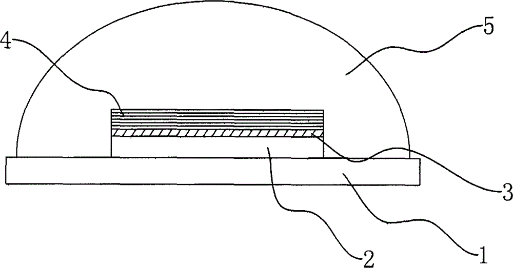
[0039] Such as figure 1 In the light-emitting diode structure shown, the light-emitting diode chip 2 adopts a blue light-emitting diode chip, the light-emitting layer 3 adopts fluorescent powder that is excited by blue light to generate yellow light, and the metal nanomaterial coating layer 4 adopts gold nanowires, and the gold nanowires are coated The thickness of the layer is 40 nm.

[0040] The preparation method is as follows:

[0041] ①Choose a suitable die-bonding glue to bond the LED chip to the base;

[0042] ② Lead out the electrodes on the light-emitting diode chip;

[0043] ③ Coating phosphor powder on the LED chip;

[0044] ④ preparing the gold nanowire coating layer on the upper surface of the light-emitting layer obtained in step ③;

[0045] ⑤ encapsulating the light-emitting diode prepared above;

[0046] ⑥ Test the photoelectric properties and parameters of the device.

Embodiment 2

[0048] Such as figure 1 In the light-emitting diode structure shown, the light-emitting diode chip 2 adopts a blue light-emitting diode chip, the light-emitting layer 3 adopts phosphor powder excited by blue light to generate green light, and the metal nanomaterial coating layer 4 adopts copper nanowires, and the copper nanowires are coated The thickness of the layer is 50 nm.

[0049] The preparation process is similar to Example 1.

Embodiment 3

[0051] Such as figure 1 In the light-emitting diode structure shown, the light-emitting diode chip 2 adopts a blue light-emitting diode chip, the light-emitting layer 3 adopts phosphor powder excited by blue light to generate red light, and the metal nanomaterial coating layer 4 adopts nickel nanowires, and the nickel nanowires are coated The thickness of the layer is 60 nm.

[0052] The preparation process is similar to Example 1.


PUM

PropertyMeasurementUnit
Thicknessaaaaaaaaaa
Thicknessaaaaaaaaaa
Thicknessaaaaaaaaaa

Abstract

The invention discloses a light emitting diode and a manufacturing method thereof. The light emitting diode device structurally comprises a base, a light emitting diode chip and a light emitting layer on the light emitting diode chip, wherein a metal nano-material coating layer is arranged on an upper surface of the light emitting layer. Since a metal nano structure has a larger specific surface area, excellent heat-conducting property is achieved; the metal nono-material is coated on the upper surface of the light emitting layer, the heat generated by the light emitting diode chip can be effectively conducted, the light emitting diode chip is prevented from being aged at high temperature, and the service life of the light emitting diode is prolonged.

Description

technical field [0001] The invention relates to a light emitting diode. The invention also relates to a method for manufacturing a light emitting diode. Background technique [0002] Light Emitting Diode (Light Emitting Diode) is a light emitting device that emits ultraviolet, visible or infrared light when a forward voltage is applied across a semiconductor p-n junction. It is a new generation of solid light source. Because of its small size, long life, low driving voltage, fast response, shock resistance, heat resistance and other characteristics, since the first light-emitting diode came out in 1964, people have not stopped the pace of research and development. With the development of light-emitting materials The development and improvement of semiconductor manufacturing process, as well as the introduction of distributed Bragg emission structure, optical microcavity and quantum well structure in the process of chip growth, have continuously improved the efficiency of li...

Claims


Application Information

Patent Timeline
IPC IPC(8): H01L33/48H01L33/64
Inventor 闭伟焕赵文强李绍荣于军胜马云辉
Owner TATWAH SMARTECH CO LTD
Why Eureka
Try Eureka