Method and apparatus for additively forming an optical component

a technology of optical components and additive manufacturing, applied in glass making apparatus, additive manufacturing, manufacturing tools, etc., can solve problems such as limiting resolution, impeded structure, and potential sidewall roughness issues

Pending Publication Date: 2022-08-11
BONSENS
View PDF0 Cites 0 Cited by
  • Summary
  • Abstract
  • Description
  • Claims
  • Application Information

AI Technical Summary

Problems solved by technology

However, the thermal and chemical stability of silica glass, together with its brittleness, impede its structuring, especially on a micrometric scale.
Each of these processes has drawbacks such as requiring multiple steps to define the waveguide, potential sidewall roughness issues, limited resolution, incompatibility with PWB manufacturing schemes and high labour costs.
Applying stereolithography to silica nanocomposites allows additive printing of silica-glass structures in 3D, but high-temperature sintering is necessary, and the minimum resolution is limited to about 60 micrometers which is still outside the relevant range for most microsystem applications.
On the other hand, the subtractive method of laser-assisted chemical etching of a silica-glass volume enables fabricating 3D components with submicrometric features, but it suffers from the very limited capability of integration and rough surface.

Method used


Image

  • Method and apparatus for additively forming an optical component
  • Method and apparatus for additively forming an optical component
  • Method and apparatus for additively forming an optical component

Examples


Embodiment Construction

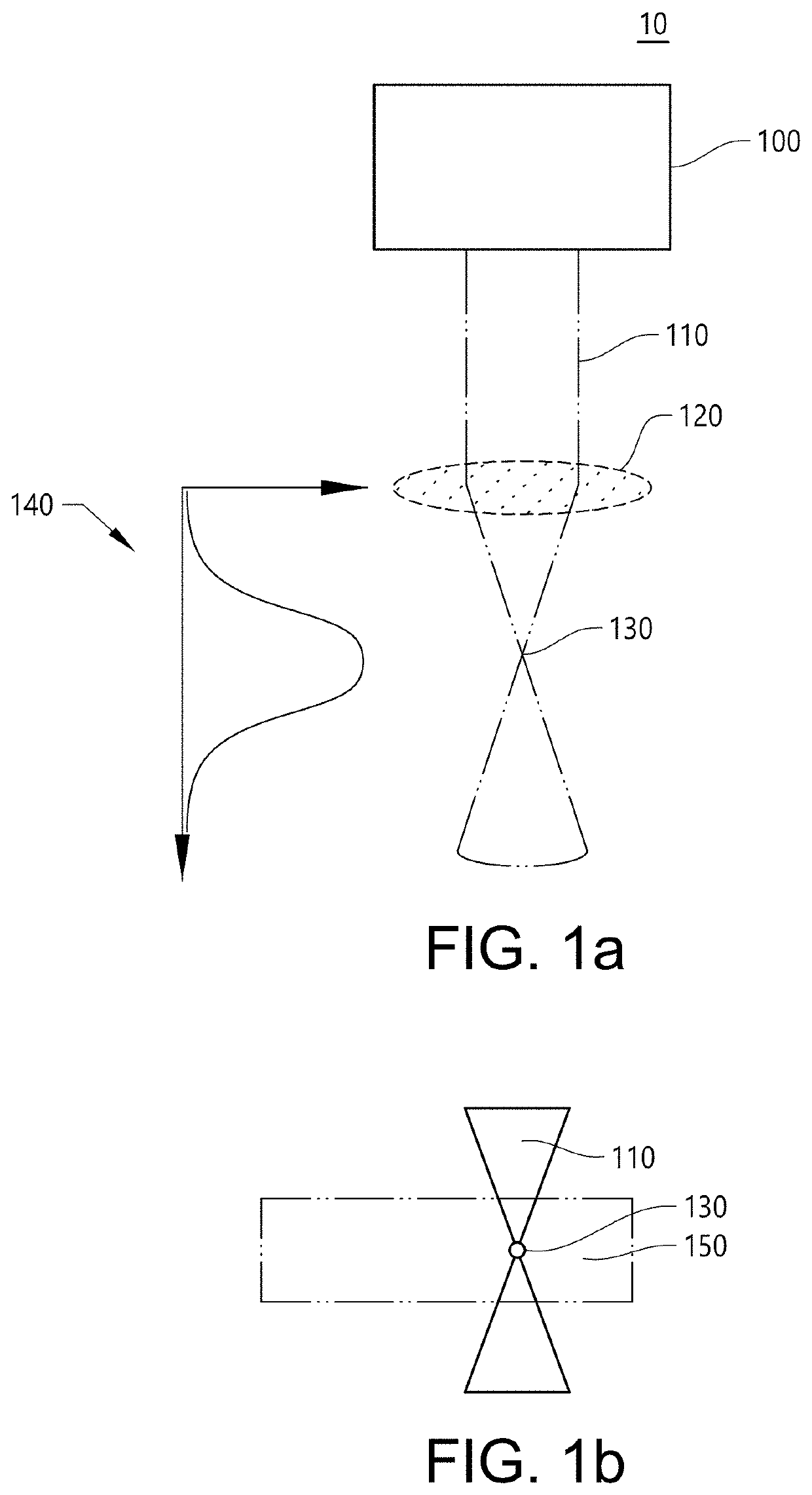
[0027]FIGS. 1a-b depicts a schematic picture of an exposure system 10 and multi-photon absorption principle. The exposure system 10 comprises a source for generating electromagnetic waves 100, a focusing lens 120 and a photo imageable layer 150. The source for generating electromagnetic waves may be a light source, for instance a femtosecond titanium sapphire laser, an argon ion-pumped laser, a colliding-pulse mode locked laser operating at frequencies from 1 Hz-100 MHz or 10 Hz-80 MHz or 100 Hz-1 MHz. The focusing lens 120 may be a single lens or a lens system. The focusing lend may be immersed in immersion oil for improved optical performance. The lens system may have fixed lenses in relation to each other or lenses with adjustable distance from each other. The lens system may be a variable focal-length lens assembly. The lens system may provide for a varying position of a focal point 130 within said photo imageable layer 150 in one or several directions. In various example embodi...


PUM

PropertyMeasurementUnit
thicknessaaaaaaaaaa
wavelengthaaaaaaaaaa
temperatureaaaaaaaaaa

Abstract

The present invention relates to a method for forming a 3D optical component comprising the steps of: forming over a substrate a liquid layer of a polymer in a solvent, drying said polymer for removing at least a portion of said solvent and thereby creating a layer having a first dissolution rate, exposing by multi-photon absorption using an electromagnetic radiation source a predefined volume of said layer, thereby causing the volume to have a second dissolution rate which is different to said first dissolution rate, dissolve the non-exposed areas with a liquid solution for forming the 3D optical component, wherein said polymer is Hydrogen silsesquioxane, HSQ, and said dried layer having a thickness of at least 1 μm.

Description

BACKGROUNDRelated Field[0001]The present invention relates in general to the field of optical components. In particular, the present invention relates to methods for forming optical components for instance waveguides, filters, optical interconnects, lenses, diffraction gratings, etc., using multi-photon absorption.Related Art[0002]Humankind has manufactured silica-glass objects for over three thousand years. Presently, silica glass is used in most branches of society, industry, and scientific research due to its excellent material properties: extreme thermal and chemical stability, excellent mechanical properties, and optical transparency in a wide wavelength range. However, the thermal and chemical stability of silica glass, together with its brittleness, impede its structuring, especially on a micrometric scale.[0003]Known methods for manufacturing optical waveguides include, for instance, manually placing glass fibers into hollowed out areas on a substrate, filling a mold of a de...

Claims


Application Information

Patent Timeline
Patent Type & Authority Applications(United States)
IPC IPC(8): C03B19/01B33Y80/00B33Y10/00B33Y30/00
CPCC03B19/01B33Y80/00H04N13/254B33Y30/00B33Y10/00C03B19/12B29C64/124H04N23/60
Inventor HUANG, PO-HANSTEMME, GÖRANNIKLAUS, FRANKGYLFASON, KRISTINN B.LAAKSO, MIKUEDINGER, PIERREHERRANZ, CARLOS ERRANDOMARSCHNER, DAVID EMMANUELLAI, LEE-LUN
Owner BONSENS
Why Eureka
Try Eureka