Defect passivation method for solving problem of luminous decay of copper-indium-gallium-selenium solar cell
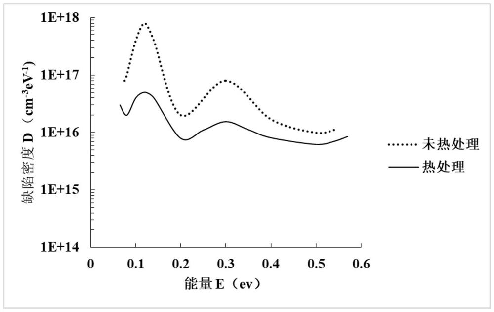
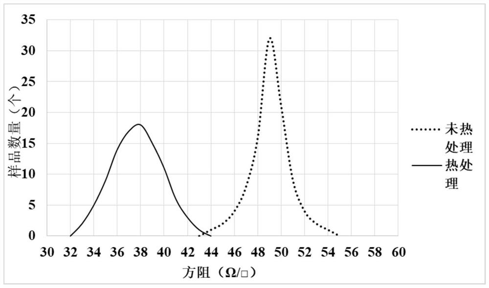
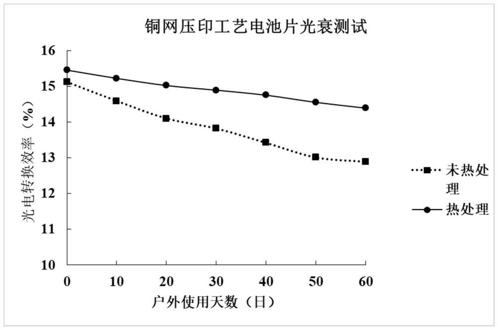
A solar cell, copper indium gallium selenide technology, applied in the direction of circuits, photovoltaic power generation, electrical components, etc., can solve the problems affecting the normal use power and expected service life of copper indium gallium selenide thin film solar cells Attenuation, battery photoelectric conversion efficiency decline and other problems, to achieve the effect of improving photoelectric conversion efficiency, reducing light attenuation, and reducing defect density
- Summary
- Abstract
- Description
- Claims
- Application Information
AI Technical Summary
Problems solved by technology
Method used
Image
Examples
Embodiment approach
[0041] A defect passivation method for solving the light decay problem of copper indium gallium selenide solar cells, comprising the following steps:
[0042] (1) Deposit the Mo back electrode on the substrate; the thickness of the Mo back electrode is 450-550nm.
[0043] (2) Deposit an alkali metal pre-layer on the Mo back electrode first, and then deposit a copper indium gallium selenium light absorption layer. The thickness of the alkali metal pre-layer is 2-20nm, and the material of the alkali metal pre-layer is selected from NaF, KF, and RbF , one of CsF. The thickness of the CIGS light absorbing layer is 1.0-3.0 μm. Depositing the copper indium gallium selenium light absorption layer adopts a three-step co-evaporation method, the first step: raise the substrate temperature to 300-450 ° C, and co-evaporate In, Ga, Se, and the deposition thickness is 0.5-1.2 μm, where 0.2≤Ga / (In+Ga)≤0.5; the second step: raise the substrate temperature to 450-650°C, co-evaporate Cu and Se...
Embodiment 1
[0052] 1. A layer of Mo back electrode with a thickness of 500nm is covered on the stainless steel substrate by magnetron sputtering.
[0053] 2. In a vacuum of 1×10 -3 The temperature of the substrate was raised to 300°C in the co-evaporation chamber of Pa, and a layer of NaF was co-evaporated on the surface of the Mo layer. The temperature of the NaF evaporation source was 765°C, and the evaporation time was 10 minutes.
[0054] The first step of deposition: raise the substrate temperature to 550°C, and co-evaporate In, Ga, and Se, where the In evaporation source temperature is 1040°C, the Ga evaporation source temperature is 1120°C, the Se evaporation source temperature is 460°C, and the evaporation time is 10min.
[0055] The second step of deposition: keep the substrate temperature constant, evaporate Cu and Se, wherein the temperature of Cu evaporation source is 1350°C, the temperature of Se evaporation source is 480°C, and the evaporation time is 20min.
[0056] The t...
Embodiment 2
[0064] 1. Cover a layer of Mo back electrode with a thickness of 500nm on the stainless steel substrate by magnetron sputtering;
[0065] 2. In a vacuum of 1×10 -3 Raise the substrate temperature to 280°C in the co-evaporation chamber of Pa, co-evaporate a NaF layer on the surface of the Mo layer, the NaF evaporation source temperature is 770°C, and the evaporation time is 10min.
[0066] The first step of deposition: raise the substrate temperature to 525°C, and co-evaporate In, Ga, and Se, where the In evaporation source temperature is 1060°C, the Ga evaporation source temperature is 1130°C, the Se evaporation source temperature is 465°C, and the evaporation time is 10min.
[0067] The second step of deposition: keep the substrate temperature constant, evaporate Cu and Se, wherein the temperature of Cu evaporation source is 1380°C, the temperature of Se evaporation source is 480°C, and the evaporation time is 19min.
[0068] The third step of deposition: keep the substrate...
PUM
| Property | Measurement | Unit |
|---|---|---|
| thickness | aaaaa | aaaaa |
| thickness | aaaaa | aaaaa |
| thickness | aaaaa | aaaaa |
Abstract
Description
Claims
Application Information


