Method of developing substructure MBE (molecular beam epitaxy) with same mass on side wall of GaAs nanowire

A sidewall growth and nanowire technology, which is applied in the fields of electrical components, semiconductor/solid-state device manufacturing, circuits, etc., can solve the problem that the optical and magnetic characterization has not been significantly developed, the density and position cannot be quantitatively controlled, electrical, Optical property crosstalk and other issues, to achieve the effect of good optical properties and single photon emission characteristics, high repeatability, and good three-dimensional confinement

Active Publication Date: 2013-06-19
INST OF SEMICONDUCTORS - CHINESE ACAD OF SCI
View PDF2 Cites 13 Cited by
  • Summary
  • Abstract
  • Description
  • Claims
  • Application Information

AI Technical Summary

Problems solved by technology

The development of quantum communication and quantum information has put forward new requirements for non-classical single-photon sources. People are also interested in the characteristics of quantum dots in the "atom-like" system, single electrons in quantum rings, and single-photon emission. Among them The design and controllable growth of microstructure is the necessary material basis, which is difficult to achieve in the traditional self-organized growth system
[0004] The preparation of quantum dots by the droplet method was proposed by Takaaki MANO et al. around 1999, and was gradually applied to the field of preparation of quantum rings in 2005. It experienced the development of quantum dots-quantum rings-coaxial multi-ring structure. The field of control has achieved great success, but so far there has been no significant development in optical and magnetic characterization, reflecting the limitations of the droplet method to prepare microstructures
At the same time, the droplet method also has the common limitation of self-organized growth, that is, its density and position cannot be quantitatively controlled. Therefore, when characterizing and studying the properties of quantum dots and nanorings, the only way to qualitatively reduce their density and use micro In the way of characterization of the region, multiple quantum units and environmental charges will cause crosstalk to its electrical and optical properties, which is very unfavorable for the isolation and preparation of a single quantum device
In addition, the traditional droplet method to prepare quantum structures is carried out on heterogeneous materials, such as lattice-matched AlAs / GaAs system and lattice-mismatched GaAs / InAs system, but it has never been formed on homogeneous materials. Examples of Quantum Structures

Method used


Image

  • Method of developing substructure MBE (molecular beam epitaxy) with same mass on side wall of GaAs nanowire
  • Method of developing substructure MBE (molecular beam epitaxy) with same mass on side wall of GaAs nanowire
  • Method of developing substructure MBE (molecular beam epitaxy) with same mass on side wall of GaAs nanowire

Examples


Embodiment Construction

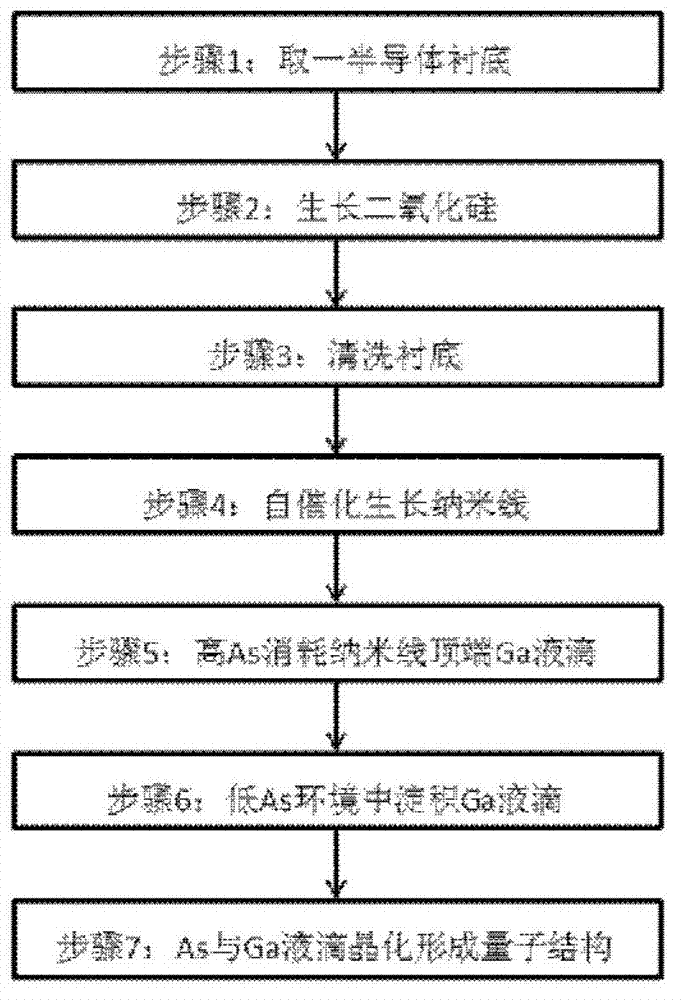
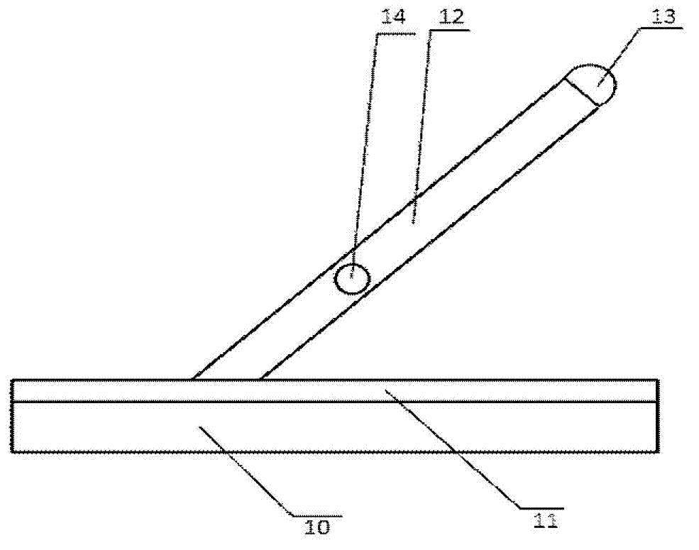
[0028] see figure 1 and figure 2 As shown, the present invention provides a kind of MBE method that grows homogeneous quantum structure on GaAs nanowire sidewall, comprises the steps:

[0029] Step 1: Take a semiconductor substrate 10, and the material of the semiconductor substrate 10 is GaAs(001) or GaAs(111)B. It should be noted that, in addition to gallium arsenide GaAs, the selected substrate material may also be semiconductor materials such as silicon Si.

[0030] Step 2: growing a silicon dioxide layer (SiO2) on the semiconductor substrate 10 2 ) 11, adopting the method of ion beam sputtering, the thickness of the silicon dioxide layer 11 is 10-20nm. Preparation of SiO 2 There are many ways of layer 11, the basic principle is to be able to precisely control the thickness of the thin layer, too thick SiO 2 Layer 11 will result in no nanowire growth on the surface or a small amount of nanowires with no fixed orientation. Grown SiO 2 Before layer 11, if the GaAs su...


PUM


Abstract

Disclosed is a method of developing substructure MBE (molecular beam epitaxy) with same mass on the side wall of GaAs nanowire. The method comprises the following steps: (1) taking a semiconductor substrate; (2) developing a silica layer on the semiconductor substrate; (3) rinsing the semiconductor substrate developed with the silica layer; (4) using a autocatalysis method, developing nanowire on the silica layer and the top end of the nanowire has a drop of Ga (gallium), (5) using high As (arsenic) pressure to process and consume the drop of Ga on the top end of the nanowire, so that the developing of VLS (Vapor Liquid Solid) of the nanowire on the top end can be restrained to form a substrate; (6) depositing the drop of Ga on the substrate under the circumstance of low As pressure; (7) under the circumstance of As, combining and crystalizing the drop of As and the drop of Ga into quantum ring or quantum dot on the side wall of the nanowire on the substrate.

Description

technical field [0001] The invention belongs to the technical field of semiconductor materials and devices, and relates to an MBE method for growing homogeneous quantum structures on the side walls of GaAs nanowires. Background technique [0002] A large part of the development of optoelectronic technology depends on the progress of micro-nano technology. Among them, nanowires, quantum dots, and quantum rings have attracted extensive attention due to their unique multi-dimensional confinement effects. It is a perfect carrier for studying magnetic properties and Aharonov-Bohm effect. [0003] Traditional quantum dots and quantum rings are mostly grown in the S-K mode or droplet method of self-organization, and have been widely used in traditional optoelectronic fields such as lasers, LEDs, and photodiodes. Their size, position, and density are usually determined by temperature, rate, etc. way to qualitatively control. The development of quantum communication and quantum inf...

Claims


Application Information

Patent Timeline
Patent Type & Authority Applications(China)
IPC IPC(8): H01L21/20
Inventor 査国伟李密锋喻颖王莉娟徐建星尚向军倪海桥贺振宏牛智川
Owner INST OF SEMICONDUCTORS - CHINESE ACAD OF SCI
Why Eureka
Try Eureka