Film-forming ink, film-forming method, method of manufacturing light emitting element, light emitting element, light emitting device, and electronic apparatus
A light-emitting element and manufacturing method technology, applied in the direction of electroluminescent light source, semiconductor/solid-state device manufacturing, ink, etc., can solve the problems of insufficient wetting and diffusion, deterioration of light-emitting element characteristics, large contact angle, etc., and achieve storage stability Excellent, excellent storage stability and desolvability, and the effect of preventing deterioration of properties
- Summary
- Abstract
- Description
- Claims
- Application Information
AI Technical Summary
Problems solved by technology
Method used
Image
Examples
no. 1 approach
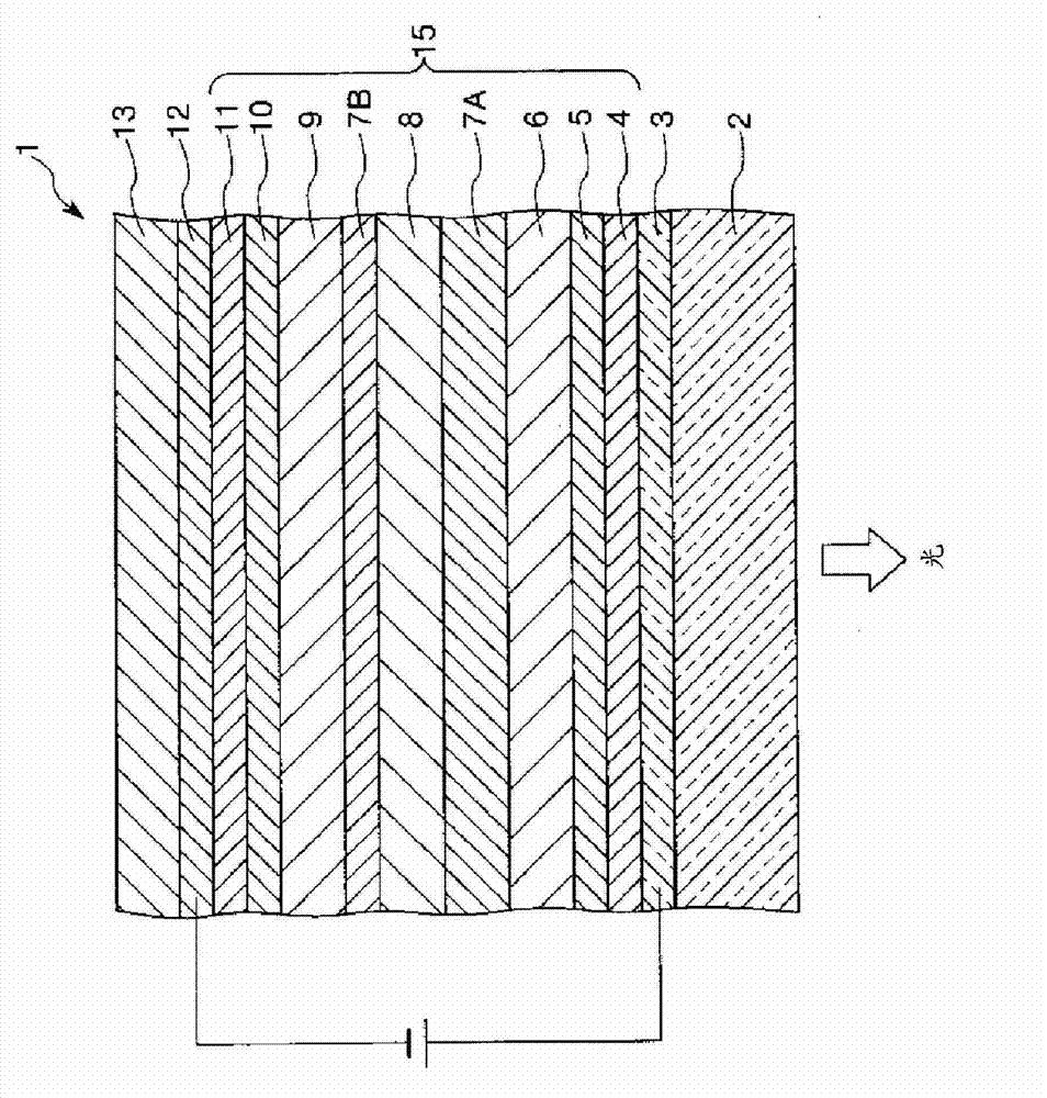
[0072] Light emitting element
[0073] figure 1 It is a figure which schematically shows the vertical cross-section of the light-emitting element of this invention. It should be explained that, for the convenience of explanation, the following figure 1 The upper side among them will be described as "upper" and the lower side as "lower".
[0074] figure 1 The light-emitting element (electroluminescent element) 1 shown emits light from R (red), G (green), and B (blue) to emit white.
[0075] This light-emitting element 1 is between the anode 3 and the cathode 12, according to the hole injection layer 4, the hole transport layer 5, the red light-emitting layer (first light-emitting layer) 6, the first intermediate layer 7A, the blue light-emitting layer ( The second light emitting layer) 8 , the second intermediate layer 7B, the green light emitting layer (third light emitting layer) 9 , the electron transport layer 10 , and the electron injection layer 11 are laminated in th...
no. 2 approach
[0296] In the second embodiment, unlike the first embodiment, the light-emitting elements may be formed as elements that emit red, green, and blue colors, respectively.
[0297]
[0298] Next, refer to Figure 8 and Figure 9 A light-emitting device including a light-emitting element produced by applying the method for producing a light-emitting element according to this embodiment will be described. Figure 8 is a schematic plan view showing the configuration of the light emitting device according to the present embodiment, Figure 9 It is a schematic sectional view of main parts showing the configuration of the light emitting device according to the present embodiment.
[0299] Such as Figure 8 As shown, the organic EL device 240 of the present embodiment includes an element substrate 201 including three-color light-emitting pixels 207 of R (red), G (green), and B (blue), and are opposed to each other at predetermined intervals on the element substrate 201 . configure...
Embodiment 1
[0370] Next, specific examples of the present invention will be described.
[0371] 1. Preparation of Liquid Medium
[0372] Liquid media (solvents) of the following samples No. 1-1 to No. 1-41 were prepared.
[0373] Sample No.1-1
[0374] With respect to 1,4-dimethylnaphthalene (bp: 268): 90 parts by mass, a compound represented by the above formula (I) (n=0, R 1 The number of carbon atoms = 2, R 2 carbon number = 2) of diethyl ether (bp: 34.6°C): 10 parts by mass of a mixed solvent
[0375] Sample No.1-2
[0376] With respect to 1,4-dimethylnaphthalene (bp: 268): 90 parts by mass, a compound represented by the above formula (I) (n=0, R 1 The number of carbon atoms = 2, R 2 carbon number = 3) ethyl propyl ether (bp: 62°C): 10 parts by mass of a mixed solvent
[0377] Sample No.1-3
[0378] With respect to 1,4-dimethylnaphthalene (bp: 268): 90 parts by mass, a compound represented by the above formula (I) (n=0, R 1 The number of carbon atoms = 3 (branch), R 2 Diisop...
PUM
| Property | Measurement | Unit |
|---|---|---|
| particle diameter | aaaaa | aaaaa |
| boiling point | aaaaa | aaaaa |
| coating thickness | aaaaa | aaaaa |
Abstract
Description
Claims
Application Information


