
NMOS (N-channel metal oxide semiconductor) device, with GaAs material growing in silicon grooves, based on ART (aspect radio trapping ) structure

A device and trench technology, applied in the field of NMOS devices, can solve the problems of difficulty in maintaining the development mode of logic and storage devices, speed, power consumption, integration, reliability limitations, etc., to achieve good device quality, reduce defects, and reduce growth The effect of temperature

Active Publication Date: 2013-06-26
INST OF SEMICONDUCTORS - CHINESE ACAD OF SCI
View PDF8 Cites 5 Cited by
  • Summary
  • Abstract
  • Description
  • Claims
  • Application Information

AI Technical Summary

Problems solved by technology

However, with the development of integrated circuit technology below the 22nm technology node, silicon (Si) integrated circuit technology is limited by a series of basic physical problems and process technology in terms of speed, power consumption, integration, reliability, etc., and Expensive production line construction and manufacturing costs make the integrated circuit industry face huge investment risks. The traditional silicon CMOS technology adopts "downsizing" to achieve smaller, faster, and cheaper logic and storage devices. The development model has been difficult to maintain

Method used


Image

  • NMOS (N-channel metal oxide semiconductor) device, with GaAs material growing in silicon grooves, based on ART (aspect radio trapping ) structure
  • NMOS (N-channel metal oxide semiconductor) device, with GaAs material growing in silicon grooves, based on ART (aspect radio trapping ) structure
  • NMOS (N-channel metal oxide semiconductor) device, with GaAs material growing in silicon grooves, based on ART (aspect radio trapping ) structure

Examples


Embodiment Construction

[0030] In order to make the object, technical solution and advantages of the present invention clearer, the present invention will be further described in detail below in conjunction with specific embodiments and with reference to the accompanying drawings.

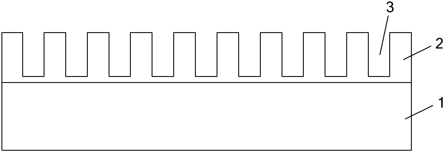
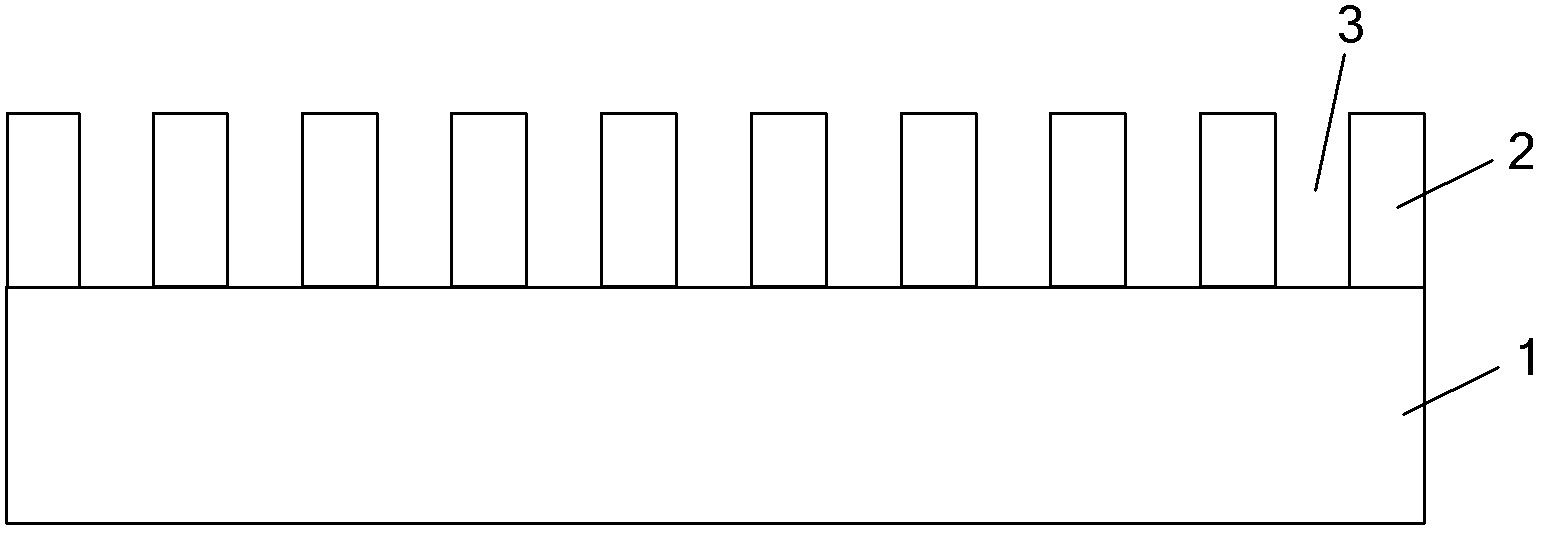
[0031] Epitaxy of high-quality III-V semiconductor materials on silicon substrates is the prerequisite for the preparation of silicon-based high-mobility NMOS. GaAs is a relatively mature III-V semiconductor material. The present invention uses GaAs as a representative of III-V semiconductor materials to study epitaxy. Al 0.3 GaAs is used as a barrier layer to obtain high-quality GaAs materials. The lattice fit of Si and GaAs is larger (4.1%), and the thermal fit is larger (the thermal expansion coefficients of Si and GaAs are 2.59×10 -6 K -1 , 5.75×10 -6 K -1 ), so there are a lot of dislocations. At the same time, due to the epitaxy of polar materials on non-polar substrates and the existence of substrate steps, a ...


PUM

PropertyMeasurementUnit
thicknessaaaaaaaaaa
widthaaaaaaaaaa

Abstract

The invention discloses a preparation method of an NMOS (N-channel metal oxide semiconductor) device and the corresponding NMOS device. The preparation method includes the steps of S1, selecting a silicon substrate which deviates 6-10 degrees in a direction from (100) to (111), and growing a SiO2 layer on the silicon substrate; S2, etching the SiO2 layer to form a plurality of grooves with aspect ratio larger than 2 on the SiO2 layer, and allowing the bottom of each groove to be exposed out of the silicon substrate; S3, under a growth pressure of 100-150 mBar, using a MOCVD (metal organic chemical vapor deposition) process to sequentially grow a barrier layer, a buffer layer and a top layer in each groove; and S4, producing a source, a drain and a grid on each top layer. Mismatch dislocation at an interface and antiphase domain boundary are stopped at a SiO2 wall, hetero-junction interface defect extension is restrained effectively, epitaxial layer quality is improved, and good device quality is achieved when an epitaxial layer is used at the substrate of the NMOS.

Description

technical field [0001] The invention relates to a method for preparing a silicon-based NMOS device and a corresponding NMOS device. Specifically, the present invention relates to the combination of MOCVD and high aspect ratio trench confinement technology (Aspect RatioTrapping, ART) to grow material structures and prepare silicon-based NMOS devices. Background technique [0002] In the past ten years, large-scale integrated circuit technology has advanced by leaps and bounds, which is largely related to the use and development of MOS transistors. Since the MOS transistor entered the integrated circuit manufacturing industry, through continuous development, it has become one of the most important electronic devices in the industry. However, the development of the electronic information industry has put forward higher requirements for integrated components. According to the prediction of the International Semiconductor Industry Technology Development Blueprint (ITRS2009), the...

Claims


Application Information

Patent Timeline
Patent Type & Authority Applications(China)
IPC IPC(8): H01L21/336H01L29/78H01L29/06
Inventor 李梦珂周旭亮于红艳李士颜米俊萍潘教青
Owner INST OF SEMICONDUCTORS - CHINESE ACAD OF SCI
Learn More