Light-emitting diode (LED) array packaging light source module based on lead frame

A technology of LED array and lead frame, which is applied in the direction of electrical components, electric solid devices, circuits, etc., can solve the problems of LED chip heat dissipation and mechanical protection, and achieve the effects of improving life, simplifying the manufacturing process, and reducing costs

Inactive Publication Date: 2013-07-03
刘胜
View PDF4 Cites 13 Cited by
  • Summary
  • Abstract
  • Description
  • Claims
  • Application Information

AI Technical Summary

Problems solved by technology

However, the current LED array packaging devices cannot meet the heat dissipation and mechanical protection requirements of LED chips.

Method used


Image

  • Light-emitting diode (LED) array packaging light source module based on lead frame
  • Light-emitting diode (LED) array packaging light source module based on lead frame
  • Light-emitting diode (LED) array packaging light source module based on lead frame

Examples


Embodiment 1

[0035] Embodiments of the present invention are further described below in conjunction with the accompanying drawings:

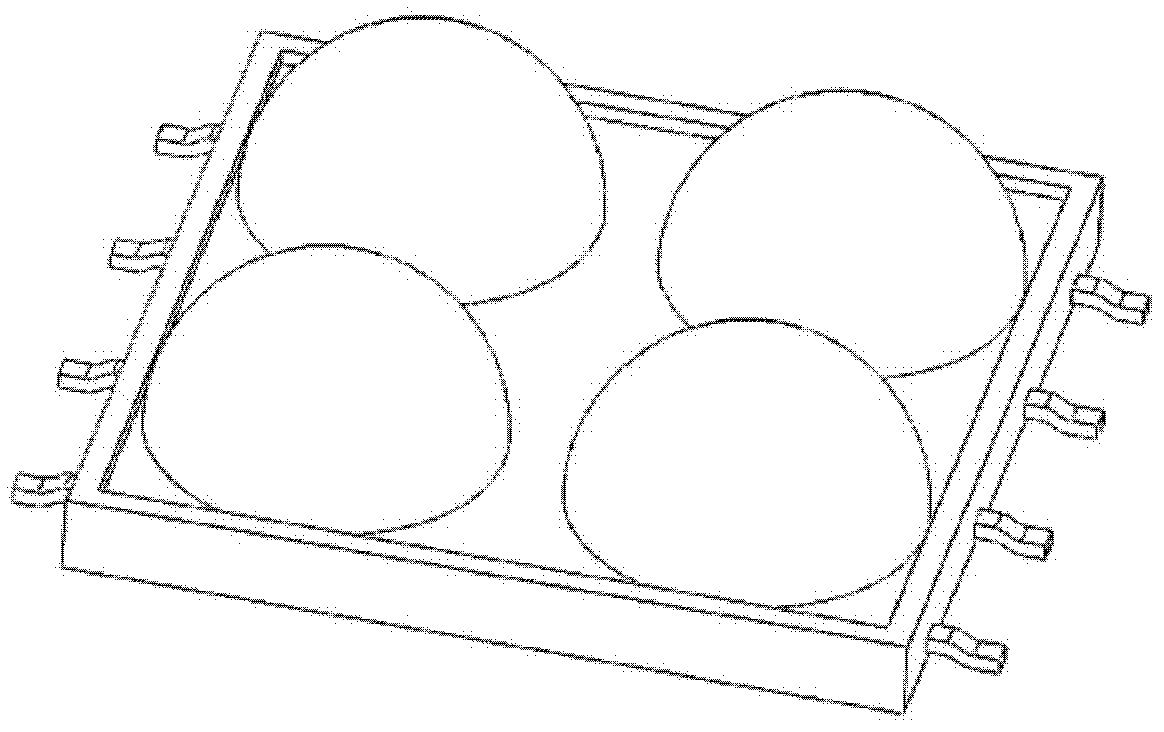
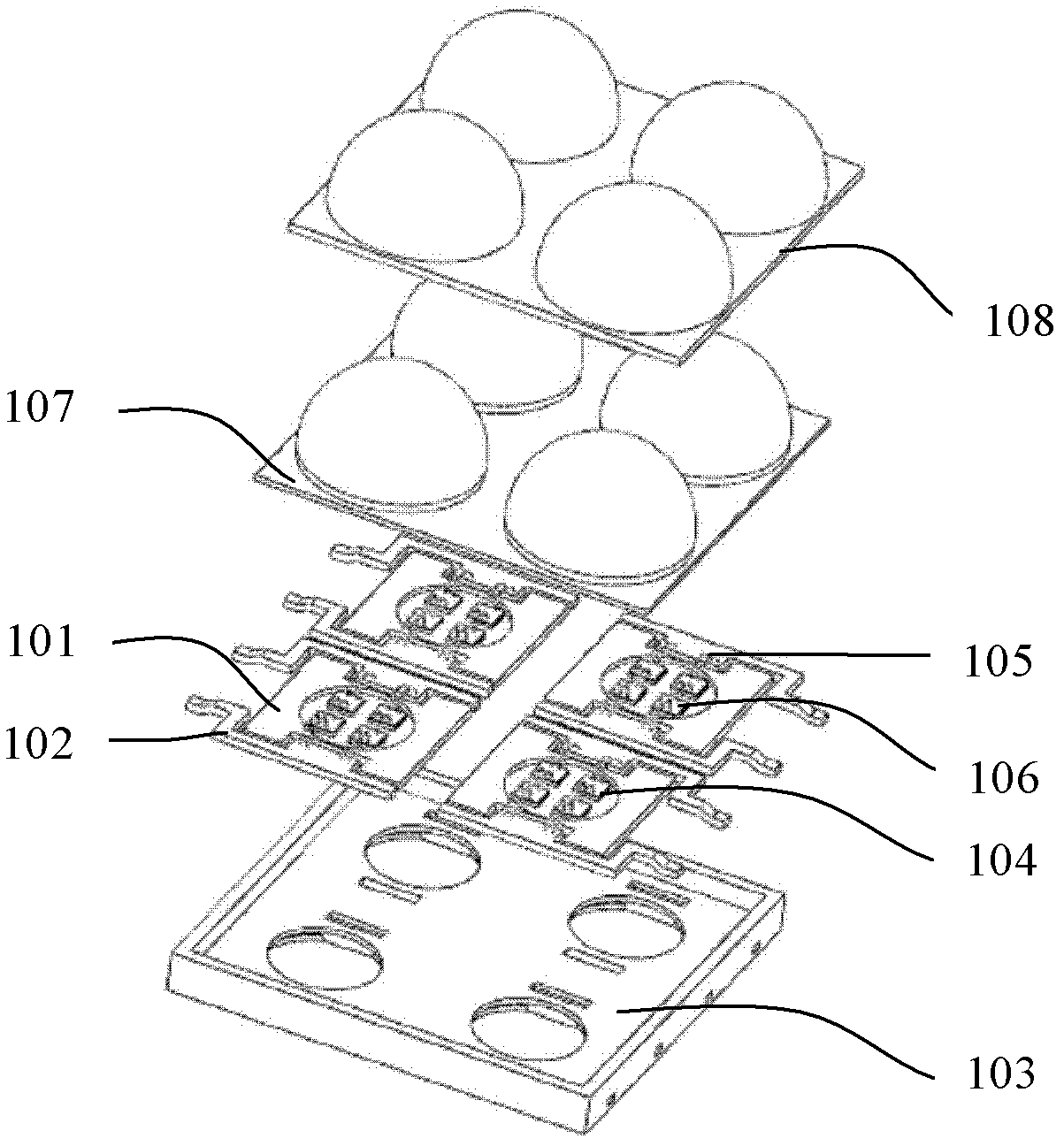
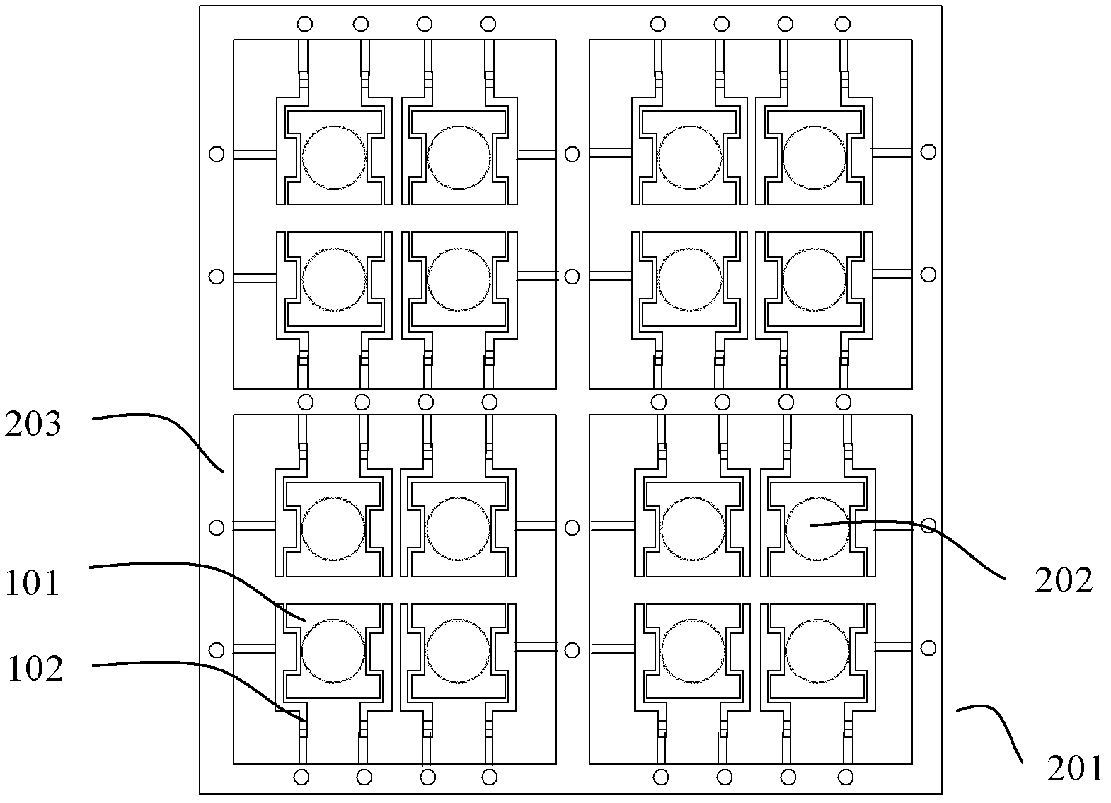
[0036] see Figure 1 to Figure 13 , this embodiment includes: a plate-shaped heat dissipation substrate 101, a lead frame 102, a molding compound 103 for insulating and providing structural support, an LED chip array 104, metal leads 105, a fluorescent powder silica gel mixture 106, silica gel 107, and an integral lens Array 108 .

[0037] The plate-shaped heat dissipation substrate 101 and the lead frame 102 are made by stamping process. The process is as follows: take a thin metal plate with a thickness of 0.1-5 mm, and make a stamping die that meets the requirements. The stamping process is carried out in two steps. The first step is to punch out a circular groove 202, and the depth of the groove is 0 -0.3 mm, the second step is stamping to separate the heat dissipation substrate 101, the lead frame 102 and the support 203. After the stamping is complet...

Embodiment 2

[0043] Embodiment 2 is the same as Embodiment 1, except that the silica gel phosphor mixture is filled into the circular groove 202 for mounting the LED chip array 104. Since the depth of the circular groove 202 is between 0-0.3 mm During this time, a uniform phosphor layer 106 is coated on the surface of the LED chip by this simple dispensing method to convert the blue light emitted by the blue LED chip into white light. It is between 20 degrees and 90 degrees.

Embodiment 3

[0045] Embodiment 3 is the same as Embodiment 1, except that the shape of the lens fixing slot is an inverted trapezoid, and the edge of the lens array 108 is an inverted trapezoid matched with it, as Figure 14 shown. The fixing of the lens array 108 is ensured through the cooperation of the inverted trapezoidal fixing slot 303, and the reliability of the LED packaging module is improved.


PUM

PropertyMeasurementUnit
Thicknessaaaaaaaaaa
Depthaaaaaaaaaa

Abstract

The invention discloses a light-emitting diode (LED) array packaging light source module based on a lead frame. The LED array packaging light source module based on the lead frame comprises an LED chip, a radiating substrate, the lead frame, a support, a molding material, fluorescent powder, potting adhesive and a lens array, and is characterized in that the LED chip is installed on the radiating substrate through welding materials, silver paste and conductive adhesive, is connected with the lead frame through a bonding wire, and is fixedly installed on molding through the radiating substrate and the lead frame in a plastic package mode, wherein the radiating substrate and the lead frame are formed by stamping thin metal plates; and a lens or the lens array is fixed on a fixed clamping groove of the molding material. The LED array packaging light source module based on the lead frame has the advantages that the lead frame and the radiating substrate are formed by once stamping the thin metal plates, manufacturing process is simple, cost can be effectively reduced, radiating performance is good, junction temperature of the LED chip is effectively reduced, service life of the LED light source is prolonged, a lens fixing device on the molding material can effectively reduce the dangers that the lens and the lens array drops, and reliability of the LED light source module is improved.

Description

technical field [0001] The invention relates to a semiconductor lighting device, in particular to an LED array packaging light source module based on a lead frame. Background technique [0002] Light-emitting diode (LED) is an electroluminescent device that can directly convert electrical energy into visible light and radiation energy. Its light-emitting mechanism is to generate photons by the recombination of electrons and holes. Compared with traditional light sources, LED has the advantages of high luminous efficiency, good color rendering, low power consumption, energy saving and environmental protection, high safety and reliability, and long service life, and has been widely used in many fields, and is considered by the industry as a lighting source The main direction of the market, with huge market potential. [0003] LED chips undergo a packaging process to form various forms of light sources. The LED package can be packaged in a single chip or an array package. Whe...

Claims


Application Information

Patent Timeline
IPC IPC(8): H01L25/075H01L33/48H01L33/62H01L33/64H01L33/58
Inventor 刘胜刘勇陈照辉宋斌王恺
Owner 刘胜
Why Eureka
Try Eureka