Manufacturing method of field blocking type semiconductor device and device structure

A manufacturing method and field blocking technology, applied in the fields of semiconductor/solid-state device manufacturing, semiconductor devices, electrical components, etc., can solve the problems such as the inability to meet the needs of activation and diffusion of the blocking layer, the limited depth of laser activation, etc., to improve the depth , the effect of improving the activation rate

Active Publication Date: 2013-07-10
SHANGHAI HUAHONG GRACE SEMICON MFG CORP
View PDF3 Cites 10 Cited by
  • Summary
  • Abstract
  • Description
  • Claims
  • Application Information

AI Technical Summary

Problems solved by technology

However, the activation depth of the laser is limited, generally only 1-2 microns, which cannot meet the needs of activation and diffusion of 3-30 micron field-blocking layers

Method used


Image

  • Manufacturing method of field blocking type semiconductor device and device structure
  • Manufacturing method of field blocking type semiconductor device and device structure
  • Manufacturing method of field blocking type semiconductor device and device structure

Examples


Embodiment 1

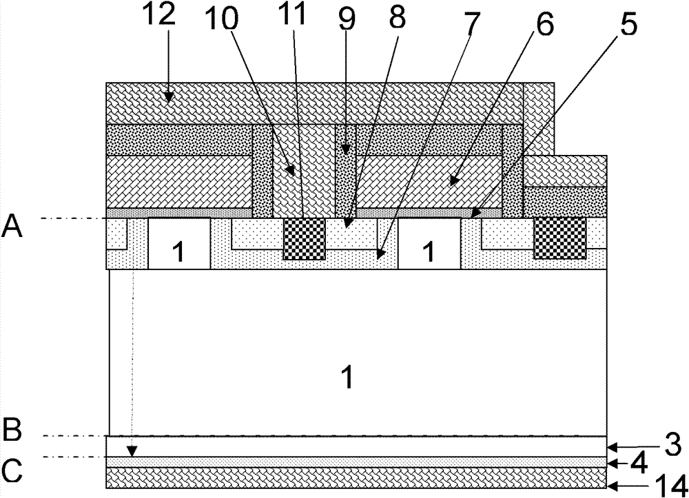
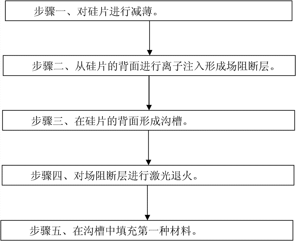
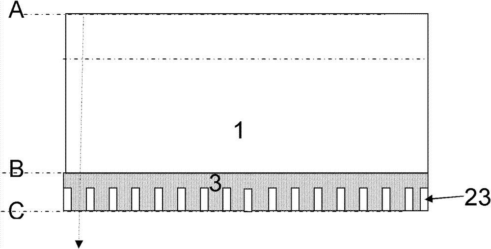
[0035] Such as figure 2 Shown is a flow chart of a method for manufacturing a field-stop type semiconductor device according to an embodiment of the present invention. The field-stop type semiconductor device in Embodiment 1 of the present invention is illustrated by taking a field-stop type IGBT device with a reverse breakdown voltage of 1200V and an N-type drift region as an example. The field-stop type IGBT with an N-type drift region The first conductivity type of the device is N-type; the method for manufacturing a field-blocking semiconductor device according to an embodiment of the present invention includes the following steps:

[0036] Step 1, such as Figure 3A As shown, first provide an impurity concentration C1 = 4.8E13CM -3 1. An N-type silicon chip 1 with a resistivity of 90 ohm.cm, and the thickness of the silicon chip 1 is more than 700 microns.

[0037] The N-type silicon wafer 1 is thinned from the back side, and the silicon wafer 1 is thinned to a requir...


PUM


Abstract

The invention discloses a manufacturing method of a field blocking type semiconductor device. According to the method, a groove is formed in the back face of a silicon wafer, so that a field blocking type layer is divided into a first field blocking layer and a second field blocking layer, the depth of the first field blocking layer is less than or equal to a first effective depth which can be reached by laser annealing, the transverse width of the second field blocking layer is twice less than or equal to the first effective depth, and accordingly the laser annealing of three dimensional directions can be conducted on the field blocking layer. Due to the laser annealing, an activation rate of the field blocking layer can be improved. Although the first effective depth of the laser annealing is only 1 micrometer-2 micrometers, the thickness of the field blocking layer is not limited by the first effective depth of the laser annealing after the method is adopted, and the depth of the field blocking layer can be improved. The invention further discloses a device structure of the field blocking type semiconductor device.

Description

technical field [0001] The invention relates to the field of semiconductor integrated circuit manufacturing, in particular to a method for manufacturing a field-stop type semiconductor device; the invention also relates to a device structure of the field-stop type semiconductor device. Background technique [0002] In semiconductor high-voltage devices, whether it is an insulated gate bipolar transistor (IGBT), a fast recovery diode (FRD), or a MOSFET, when the gate of the device is positively biased, the device is turned on. The power consumption is the smallest, that is, the on-state voltage drop of the device is expected to be small, and the on-state voltage drop of the device can be directly reduced by using a thinner silicon chip, but the decrease in the thickness of the device will reduce the reverse breakdown of the device. Under the condition of pressure resistance, the two are a pair of contradictions. In order to solve the above contradictions, the field blocking ...

Claims


Application Information

Patent Timeline
Patent Type & Authority Applications(China)
IPC IPC(8): H01L21/329H01L21/331H01L21/336H01L21/324H01L29/739H01L29/78H01L29/861
Inventor 肖胜安
Owner SHANGHAI HUAHONG GRACE SEMICON MFG CORP
Why Eureka
Try Eureka