A method for preparing a protective coating on the surface of a plasma etching chamber

A protective coating and plasma technology is applied in the field of preparation of protective coatings on the surface of ion etching chambers, which can solve the problems of unusable polymers, reduced quality of finished wafers, plasma pollution, etc., and achieves enhanced mechanical properties and chemical properties. Stability, maintain structural stability, improve the effect of anti-degeneration

Active Publication Date: 2014-10-22
INST OF METAL RESEARCH - CHINESE ACAD OF SCI
View PDF4 Cites 0 Cited by
  • Summary
  • Abstract
  • Description
  • Claims
  • Application Information

AI Technical Summary

Problems solved by technology

The film layer prepared by passivation or coating method is relatively thin, and under the continuous plasma energy bombardment, the surface of the cavity is corroded or accumulated into polymer, and finally cannot be used
[0004] Because the chemical activity of the plasma used in the etching process is strong, and the ion bombardment effect is obvious, if the chamber material has poor resistance to this type of plasma corrosion, it will bring plasma pollution, affect the etching process, and reduce the quality of the finished wafer. quality

Method used


Image

  • A method for preparing a protective coating on the surface of a plasma etching chamber
  • A method for preparing a protective coating on the surface of a plasma etching chamber
  • A method for preparing a protective coating on the surface of a plasma etching chamber

Examples


Embodiment 1

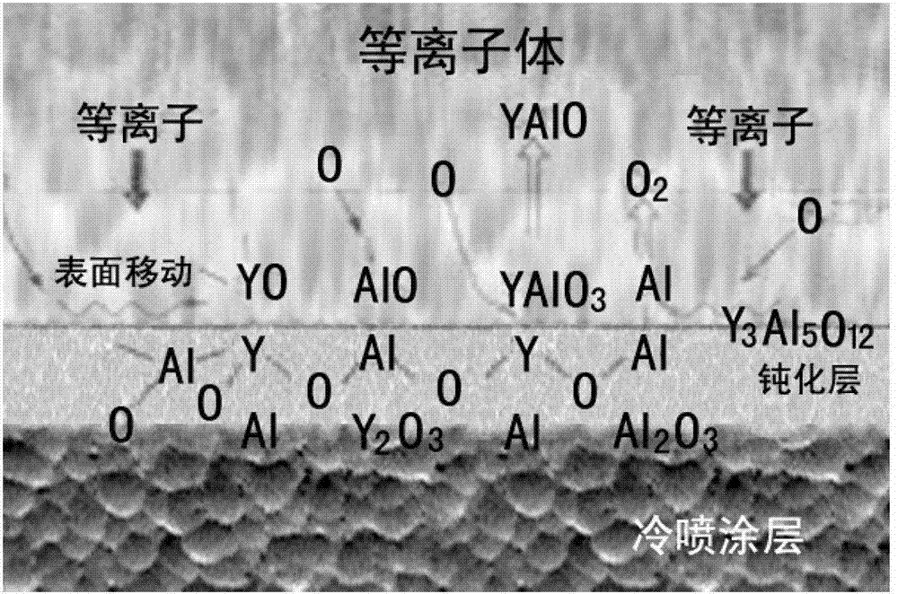
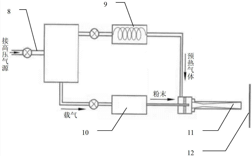
[0048] Using pure Al powder and Y 2 o 3 -A1 2 o 3 The mixed powder of the powder prepares the protective coating on the surface of the plasma etching chamber, and the Al powder and the Y 2 o 3 -A1 2 o 3 The mixed powder of the powder is directly sprayed on the surface of the ion etching chamber. By controlling the spraying parameters: the spray distance is 20mm, the gas pressure is 2.0MPa, the gas temperature is 400°C, the air flow rate is 20g / s, and the average particle size of the powder is 20μm. Deposited on the surface of the plasma etching chamber to form a uniformly distributed protective coating; among them, pure Al powder and Y 2 o 3 -A1 2 o 3 The weight ratio of powder is 0.2:1; Y 2 o 3 -A1 2 o 3 In powder, Y 2 o 3 with A1 2 o 3 The weight ratio is 2:1.

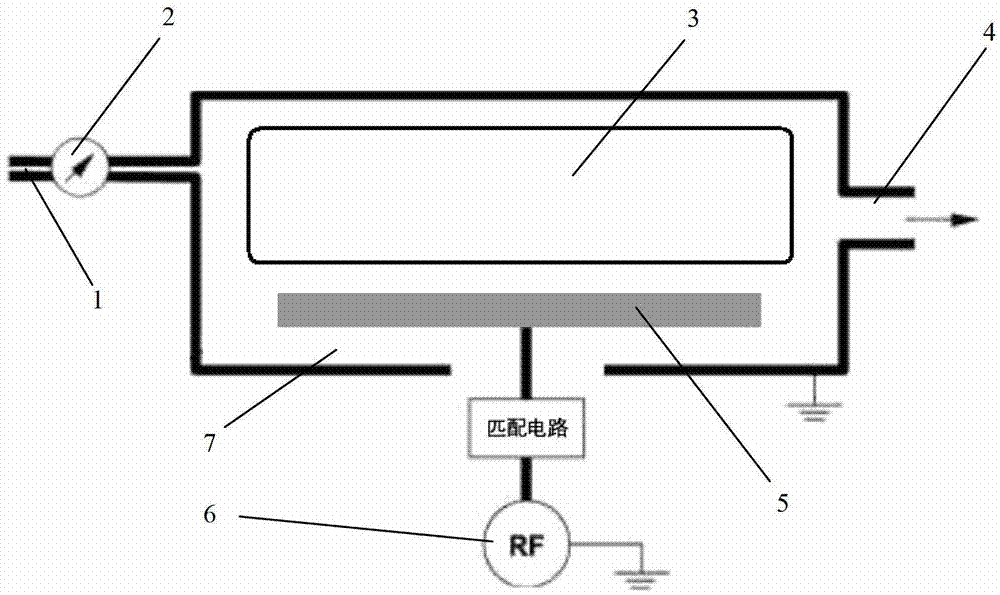
[0049] In this embodiment, the passivation process of the plasma etching chamber refers to the plasma etching process, and the passivation process conditions are as follows,

[0050] (1) Time param...

Embodiment 2

[0065] The difference from Example 1 is that

[0066] Using pure Al powder and Y 2 o 3 -A1 2 o 3 The mixed powder of the powder prepares the protective coating on the surface of the plasma etching chamber, and the Al powder and the Y 2 o 3 -A1 2 o 3 The mixed powder of the powder is directly sprayed on the surface of the ion etching chamber. By controlling the spraying parameters: the spray distance is 5mm, the gas pressure is 1.0MPa, the gas temperature is 300°C, the air flow rate is 10g / s, and the average particle size of the powder is 5μm. Deposited on the inner surface of the plasma etching chamber to form a uniformly distributed protective coating; among them, pure Al powder and Y 2 o 3 -A1 2 o 3 The weight ratio of powder is 0.6:1; Y 2 o 3 -A1 2 o 3 In powder, Y 2 o 3 with A1 2 o 3 The weight ratio is 2.2:1.

[0067] In this embodiment, doped Y 3 A1 5 o 12 thin film, doped Y 3 A1 5 o 12 film, Y 3 A1 5 o 12 Accounting for 95wt%, the rest is Y ...

Embodiment 3

[0069] The difference from Example 1 is that

[0070] Using pure Al powder and Y 2 o 3 -A1 2 o 3 The mixed powder of the powder prepares the protective coating on the surface of the plasma etching chamber, and the Al powder and the Y 2 o 3 -A1 2 o 3 The mixed powder of the powder is directly sprayed on the surface of the ion etching chamber. By controlling the spraying parameters: the spray distance is 30mm, the gas pressure is 3.0MPa, the gas temperature is 500°C, the air flow rate is 30g / s, and the powder particle size is 30μm, so that the mixed powder is deposited On the inner surface of the plasma etching chamber, a uniformly distributed protective coating is formed; among them, pure Al powder and Y 2 o 3 -A1 2 o 3 The weight ratio of powder is 1:1; Y 2 o 3 -A1 2 o 3 In powder, Y 2 o 3 with A1 2 o 3 The weight ratio is 2.3:1.

[0071] In this embodiment, doped Y 3 A1 5 o 12 thin film, doped Y 3 A1 5 o 12 film, Y 3 A1 5 o 12 Accounting for 98wt%,...


PUM

PropertyMeasurementUnit
thicknessaaaaaaaaaa
thicknessaaaaaaaaaa

Abstract

The invention relates to the field of semiconductor integrated circuit chip (wafer) plasma etching, and particularly relates to a method for preparing a protective coating layer for the surface of a plasma etched cavity. The method comprises the steps of: preparing the protective coating layer for the surface of the plasma etched cavity by adopting mixed powder of pure Al powder and Y2O3-Al2O3 powder, directly spray-coating the mixed powder of pure Al powder and Y2O3-Al2O3 powder onto the surface of an ion etched cavity by high-speed jet streams, and depositing the mixed powder on the inner surface of the plasma etched cavity by means of controlling spray-coating parameters of jetting distance to be 5-50mm, gas pressure to be 0.5-5.0MPa, gas temperature to be 260-520 DEG C, gas flow-rate to be 10-30g / s and powder particle size to be 1-50 micro meters, thus forming the evenly-distributed protective coating layer which can be passivated on site in the plasma etched cavity. By virtue of the protective coating layer, the corrosion to the cavity caused by corrosive gas and the pollution to a semiconductor wafer caused by metal ions can be reduced, and the service life of a cavity material of a reaction chamber in the production of a plasma etched wafer can be prolonged.

Description

technical field [0001] The invention relates to the field of plasma etching of semiconductor integrated circuit chips (wafers), in particular to a method for preparing a protective coating on the surface of a plasma etching chamber. Background technique [0002] Plasma etching (also known as dry etching) is one of the key processes in integrated circuit manufacturing, and its process level will directly affect the quality of the final product and the advancement of the production process. The plasma used for etching is produced by a chemically active gas. Under low pressure, the reactive gas is excited by radio frequency power to generate ionization and form a plasma. The gas in the reaction chamber forms a large amount of reactive gas under the impact of electrons. The radicals, active groups and the etched wafer or chip form a chemical reaction to form volatile reaction products, which are detached from the surface of the wafer and drawn out of the cavity. [0003] The ge...

Claims


Application Information

Patent Timeline
Patent Type & Authority Patents(China)
IPC IPC(8): C23C4/10H01L21/3065C23C24/08
Inventor 吴杰金花子沈艳芳李鸣熊天英
Owner INST OF METAL RESEARCH - CHINESE ACAD OF SCI
Why Eureka
Try Eureka