Manufacturing method of polycrystalline silicon layer and polycrystalline silicon thin film transistor and manufacturing method thereof

A technology of polysilicon thin film and polysilicon layer, which is applied in transistors, semiconductor/solid-state device manufacturing, semiconductor devices, etc., and can solve the problems of poor uniformity of polysilicon layer, grain boundary defects, uneven grains, etc.

Active Publication Date: 2013-07-24
BOE TECH GRP CO LTD +1
View PDF3 Cites 18 Cited by
  • Summary
  • Abstract
  • Description
  • Claims
  • Application Information

AI Technical Summary

Problems solved by technology

The inventors have found that the existing method has at least the following problems: there are many defects (such as grain boundary defects, uneven grains, etc.) generated during the

Method used


Image

  • Manufacturing method of polycrystalline silicon layer and polycrystalline silicon thin film transistor and manufacturing method thereof
  • Manufacturing method of polycrystalline silicon layer and polycrystalline silicon thin film transistor and manufacturing method thereof
  • Manufacturing method of polycrystalline silicon layer and polycrystalline silicon thin film transistor and manufacturing method thereof

Examples


Embodiment

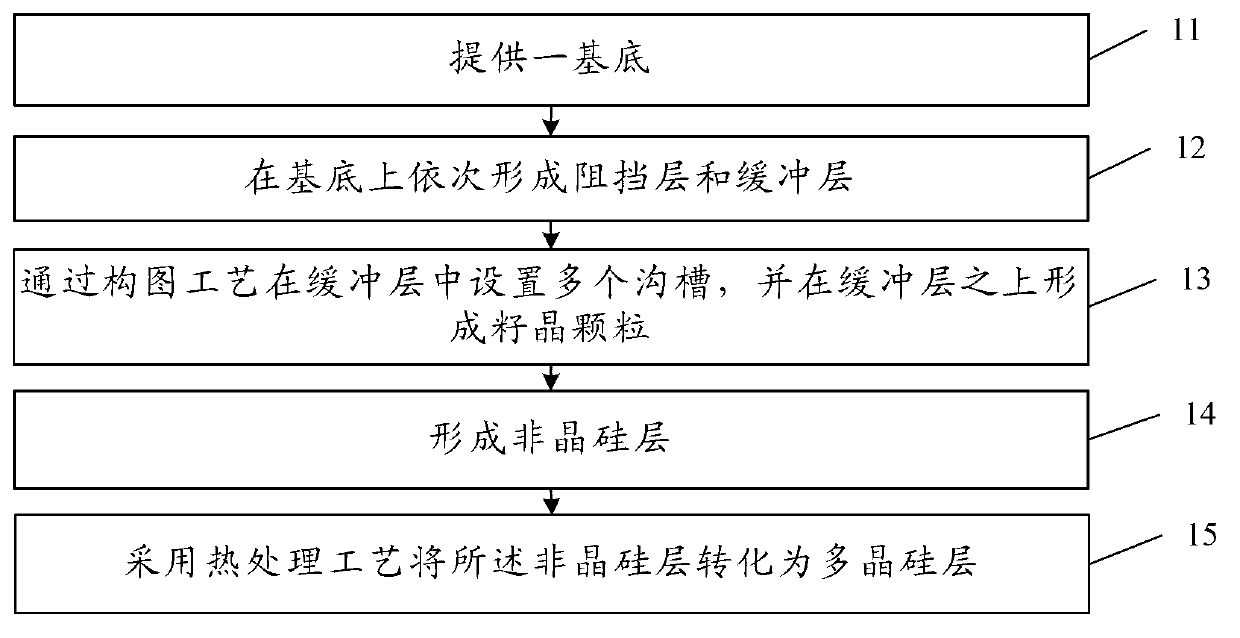
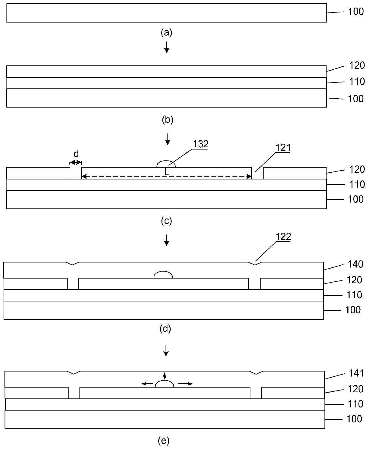
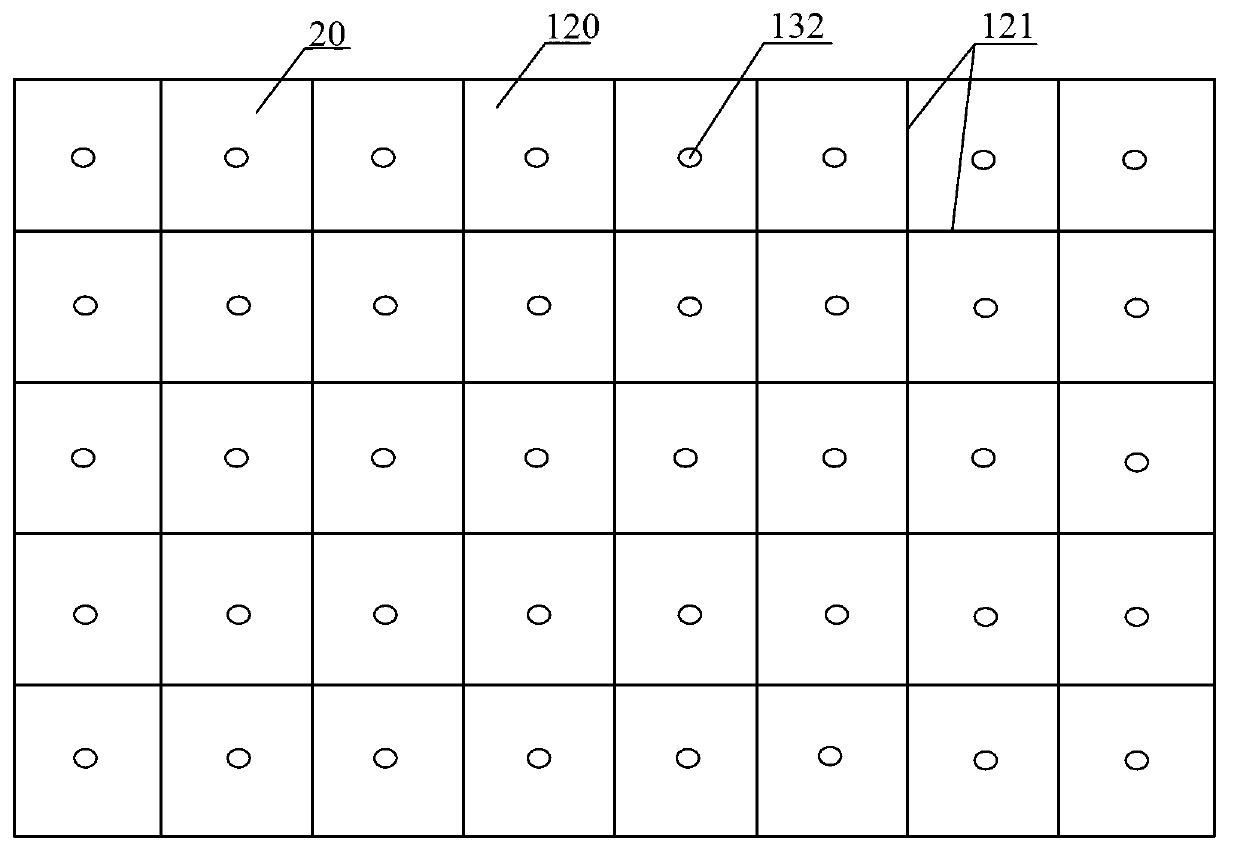
[0056] An embodiment of the present invention provides a method for manufacturing a polysilicon layer, such as figure 1 and figure 2 As shown, the method includes:

[0057] 11. Provide a substrate 100;

[0058] In this step, the substrate 100 is cleaned, and the substrate 100 may be a glass substrate or others.

[0059] 12. If figure 2 As shown in (b), a barrier layer 110 and a buffer layer 120 are sequentially formed on the substrate 100;

[0060]The barrier layer 110 is disposed between the substrate 100 and the buffer layer 120. When a trench is subsequently formed on the buffer layer 120, the barrier layer 110 can be used to prevent the substrate 100 from being etched. In practice, the buffer layer can also be formed directly on the substrate 100. 120, the barrier layer 110 is omitted.

[0061] Optionally, in this step, the barrier layer 110 and the buffer layer 120 are successively deposited on the substrate 100 using an enhanced chemical vapor deposition (PECVD) m...


PUM

PropertyMeasurementUnit
Thicknessaaaaaaaaaa

Abstract

The invention discloses a manufacturing method of a polycrystalline silicon layer and a polycrystalline silicon thin film transistor and a manufacturing method thereof, and relates to the field of displaying. According to the manufacturing methods, a crystallization rate of a formed polycrystalline silicon layer is high, crystalline grains are uniform, crystal boundary defects are little, thus electrics properties of the polycrystalline silicon thin film transistor can be improved, and reliability of the polycrystalline silicon thin film transistor is improved. The manufacturing method of the polycrystalline silicon layer includes the steps that a substrate is provided; a barrier layer and a buffer layer are sequentially formed on the substrate; multiple groves are arranged in the buffer layer through a picture composition process, and seed crystals are formed on the buffer layer; an amorphous silicon layer is formed on the buffer layer provided with the grooves and the seed crystals; and the amorphous silicon layer is converted into the polycrystalline silicon layer through adoption of a heating processing process. The manufacturing method of the polycrystalline silicon layer and the polycrystalline silicon thin film transistor and the manufacturing method of the polycrystalline silicon thin film transistor are used for improving quality of polycrystalline silicon films.

Description

technical field [0001] The present invention relates to the display field, in particular to a method for manufacturing a polysilicon layer, a method for manufacturing a polysilicon thin film transistor, a polysilicon thin film transistor formed by the method, an array substrate provided with the polysilicon thin film transistor, and a display device. Background technique [0002] Existing displays are mostly based on amorphous silicon (a-si), that is, thin film transistors (Thin Film Transistor, TFT) on the display panel mostly use amorphous silicon semiconductor materials, but in comparison, polysilicon (Poly-Si) has Higher electron mobility is considered to be a better TFT material than amorphous silicon. [0003] At present, when preparing a polysilicon TFT, a layer of amorphous silicon is usually prepared first; then the amorphous silicon layer is converted into a polysilicon layer by using an excimer laser crystallization (ELA) method; finally, a thin film transistor is...

Claims


Application Information

Patent Timeline
IPC IPC(8): H01L21/20H01L21/336H01L29/786H01L27/12
CPCH01L29/786H01L21/20H01L21/02532H01L21/02667H01L27/1288H01L21/02686H01L27/1281H01L27/1277H01L21/02592H01L21/02642H01L21/02645H01L21/02675H01L21/02694H01L21/30604H01L21/3081H01L21/3083H01L29/04H01L29/16H01L29/6675H01L29/78672
Inventor 王祖强
Owner BOE TECH GRP CO LTD
Why Eureka
Try Eureka