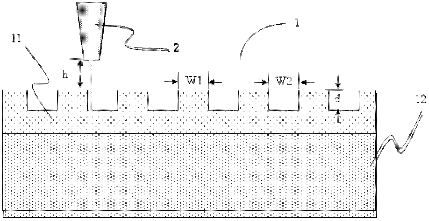
Manufacturing method for roughened transparent conducting base plate
A technology of transparent conduction and manufacturing methods, which is applied in the fields of final product manufacturing, sustainable manufacturing/processing, circuits, etc. It can solve the problems of large variability in wet etching process, difficulty in controlling the same process and etching effect, and difficulty in controlling etching patterns, etc.
- Summary
- Abstract
- Description
- Claims
- Application Information
AI Technical Summary
Problems solved by technology
Method used
Image
Examples
Embodiment 1
[0036] First, put the glass substrate into an ultrasonic oscillator and shake it with alcohol for 10 minutes. The main purpose is to remove excess organic and non-organic substances on the glass surface. Then put it into pure water and shake it for 10 minutes to remove the residue on the surface of the glass substrate. Alcohol, and then use a nitrogen gun to dry the moisture on the surface of the glass substrate, blow off the excess moisture on the surface of the glass substrate, and finally place the glass substrate in a plasma cleaning machine (O2-Plasma), and pump the cavity to a certain vacuum value , Passing an electric current produces plasma (Plasma). Clean in medium power mode for 5 minutes to remove the oxide layer or thick carbonized layer, and activate the indium tin oxide (ITO) on the glass surface to avoid excessive oxygen residue and affect the entire preparation process.
[0037] A radio frequency (RF) magnetron sputtering machine is used to deposit an indium ti...
Embodiment 2
[0042] Embodiment 2 is roughly the same as Embodiment 1. The main difference is that a 150-nm thick film of indium tin oxide (ITO) is sputtered on the glass substrate for laser engraving. The roughened transparent conductive substrate 1 produced has a light transmittance of 93.54%, the short-circuit current of the amorphous silicon thin-film solar cell increased from 8.83mA / cm2 to 9.48mA / cm2, and the efficiency increased from 4.32% to 4.86%. The efficiency of battery components is increased by about 7%.
Embodiment 3
[0044] Embodiment 3 is roughly the same as Embodiment 1. The main difference is that a 200-nanometer thick film of indium tin oxide (ITO) is sputtered on the glass substrate for laser engraving. The roughened transparent conductive substrate 1 produced has a light transmittance of 92.84%, the short-circuit current of the manufactured amorphous silicon thin-film solar cell is increased from 8.77mA / cm2 to 9.1mA / cm2, and the efficiency is increased from 3.74% to 4.56%. The efficiency of the battery module is increased by about 3.8%.
PUM
| Property | Measurement | Unit |
|---|---|---|
| depth | aaaaa | aaaaa |
| thickness | aaaaa | aaaaa |
| power | aaaaa | aaaaa |
Abstract
Description
Claims
Application Information
