

Variable-cycle multi-beam interference photoetching method
A multi-beam interference and lithography technology, which is applied in the field of nano-processing, can solve problems such as complex optical paths and difficult adjustment of beam incident angles, and achieve the effect of simple optical paths, easy pattern cycles, and large-area multi-beam interference lithography
- Summary
- Abstract
- Description
- Claims
- Application Information
AI Technical Summary
Problems solved by technology
Method used
Image

Examples
Embodiment 2
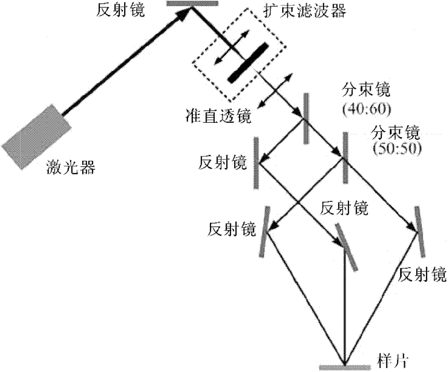
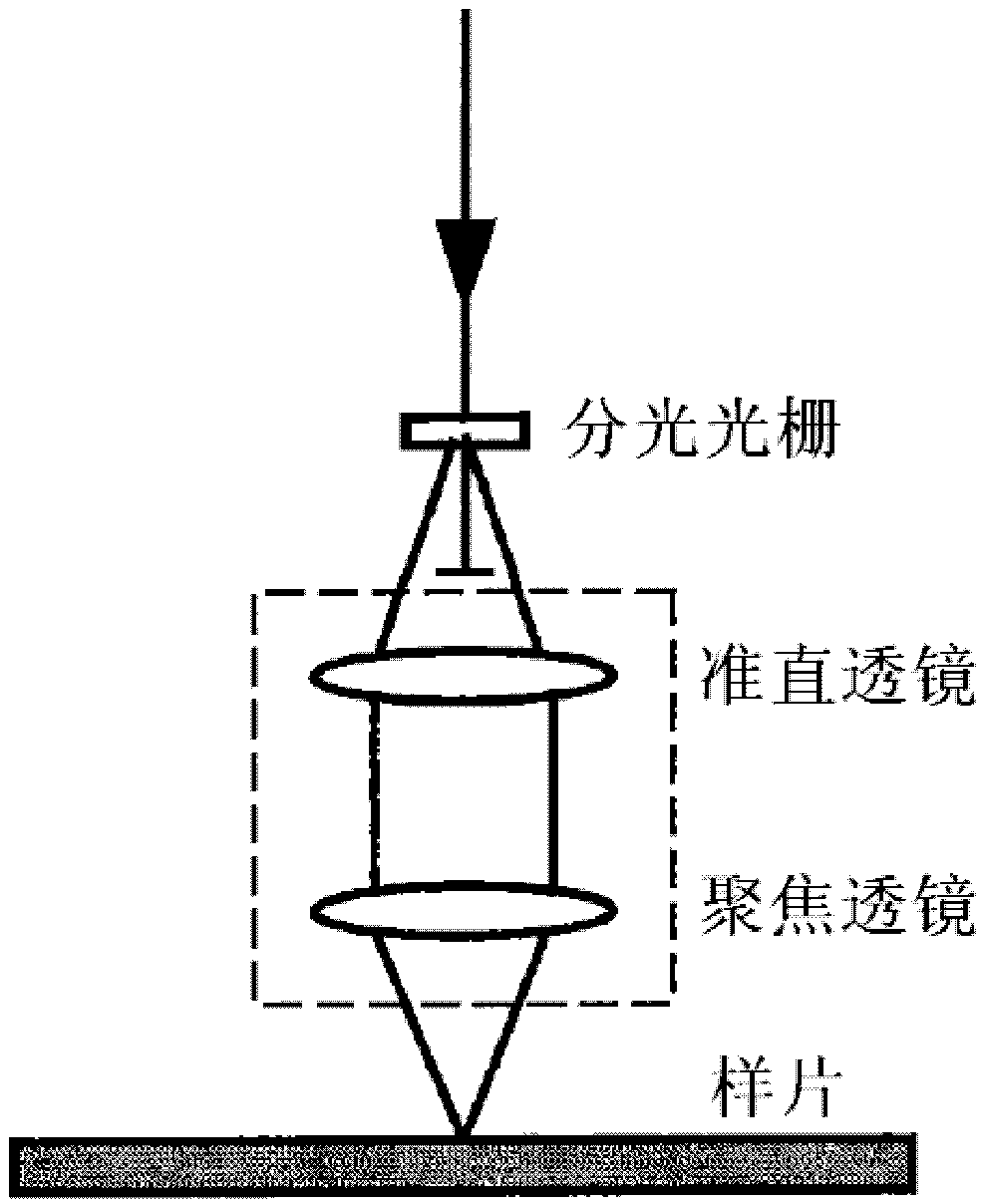
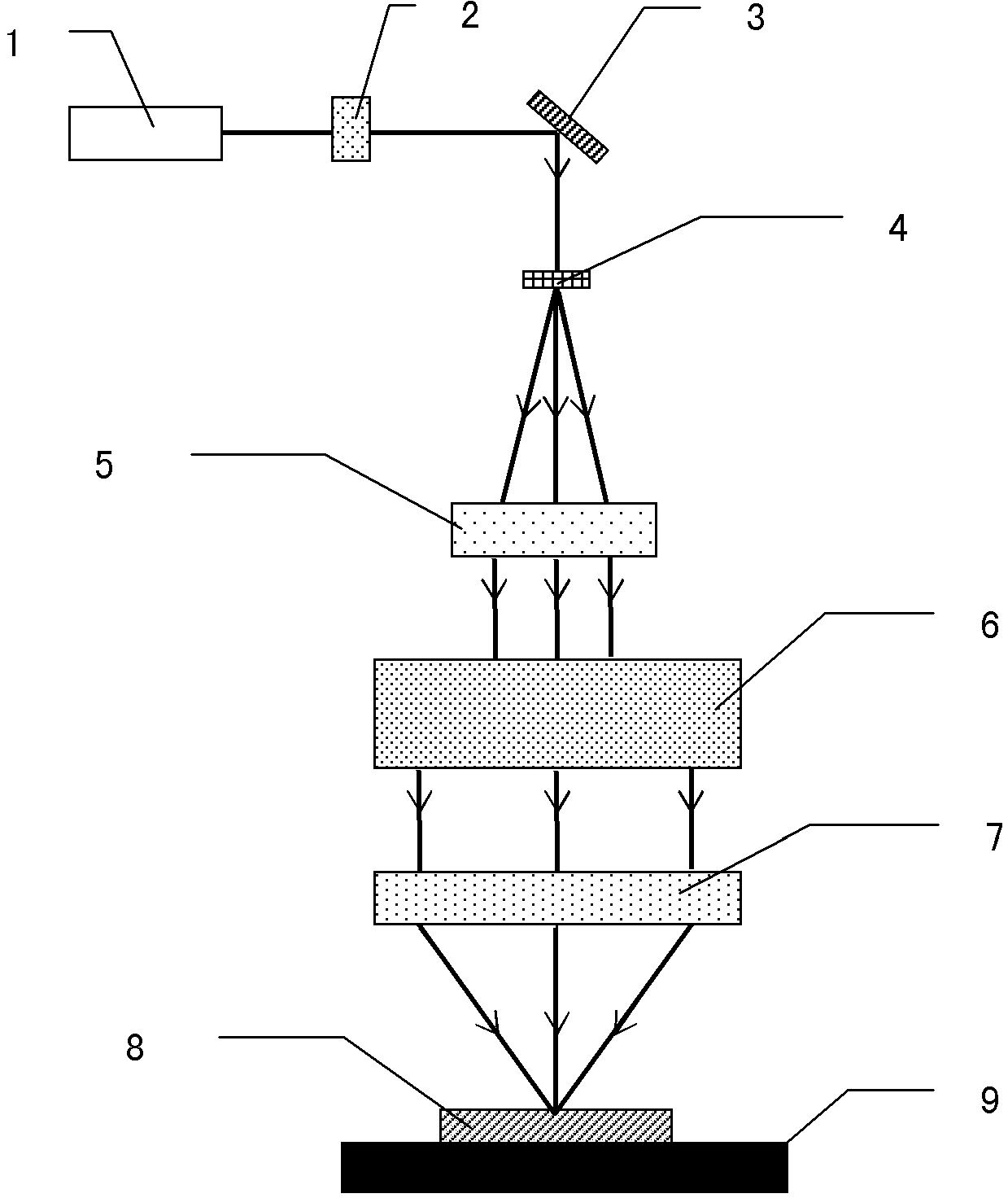
[0040] Embodiment 2 of the present invention is a four-beam interference lithography system capable of adjusting the period in the range of 656 nm to 1.94 μm.
[0041]In this system, the ultraviolet laser 1 is an argon ion laser with an output wavelength of 363.8nm, and the light splitting element 4 is a four-beam light splitting element, which is a phase diffractive optical element, and the first-order light diffraction angle is 10°. With regard to the rotational symmetry of the optical axis, the focal length of the collimator lens 5 is 25 mm, and the aperture is 12.5 mm. The incident aperture of the continuous zoom beam expander 6 is 10 mm, and the output aperture is 30 mm. times, the focal length of the focusing lens 7 is 50 mm, the aperture is 30 mm, and the numerical aperture is 0.3.
[0042] Place the light splitting element 4 at the focal point of the collimating lens 5, the laser beam is symmetrically divided into four beams by the light splitting element 4 after shapi...
PUM
 Abstract
Description
Claims
Application Information