High-robustness P type symmetric laterally double-diffused field effect transistor

A field effect transistor, lateral double diffusion technology, applied in semiconductor devices, electrical components, circuits, etc., can solve the problems of increasing device area, increasing process version complexity, decreasing current capacity, etc., reducing Joule heat, two The effect of increasing the secondary collapse current and improving the insufficient electrostatic discharge capacity

Inactive Publication Date: 2013-09-04
SOUTHEAST UNIV
View PDF5 Cites 11 Cited by
  • Summary
  • Abstract
  • Description
  • Claims
  • Application Information

AI Technical Summary

Problems solved by technology

There are many similar methods, and they also have shortcomings under the condition of improving ESD protection capabilities, such...

Method used


Image

  • High-robustness P type symmetric laterally double-diffused field effect transistor
  • High-robustness P type symmetric laterally double-diffused field effect transistor
  • High-robustness P type symmetric laterally double-diffused field effect transistor

Examples


Embodiment Construction

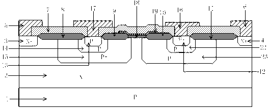
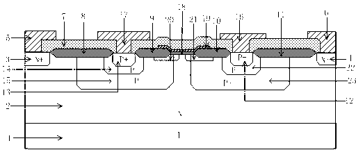
[0019] Attached below figure 2, the present invention is described in detail, a highly robust P-type symmetrical lateral double-diffused field effect transistor, comprising: a P-type substrate 1, an N-type epitaxial layer 2 is arranged on the P-type substrate 1, and an N-type epitaxial layer 2 is arranged on the N-type The inside of the epitaxial layer 2 is provided with a first P-type drift well 15 and a second P-type drift well 23, and a first P-type buffer well 14 is arranged inside the first P-type drift well 15, and a second P-type drift well 23 is provided with a second P-type buffer well 22, a P-type source region 13 is provided in the first P-type buffer well 14, a P-type drain region 12 is provided in the second P-type buffer well 22, and a P-type drain region 12 is provided in the N-type buffer well 14. The inside of the epitaxial layer 2 is also provided with a first N-type body contact region 3 and a second N-type body contact region 4, and on the surface of the N...


PUM


Abstract

The invention discloses a high-robustness P type symmetric laterally double-diffused field effect transistor, which comprises a P type substrate, wherein an N type epitaxial layer is arranged on the P type substrate; two P type drift traps, two P type buffer traps and two N type body contact regions are arranged in the N type epitaxial layer; a P type drain region and a P type source region are arranged in the P type buffer trap respectively; the surface of the N type epitaxial layer is provided with a gate oxide layer and a field oxide layer; the surface of the gate oxide layer is provided with a polycrystalline silicon gate; the surfaces of the field oxide layer, the N type body contact regions, the P type source region, the polycrystalline silicon gate and the P type drain region are provided with passivation layers; the high-robustness P type symmetric laterally double-diffused field effect transistor is characterized in that the surfaces of the two P type drift traps are also provided with a photo-etching plate shared with the low-voltage P type trap; first and second shallow P type traps formed by low-energy ion implantation are adopted; and the surface electric field distribution is effectively optimized at the region, the highest lattice temperature is reduced, the secondary breakdown current is improved and the robustness of the device in an ESD (Electronic Static Discharge) process is enhanced.

Description

technical field [0001] The invention mainly relates to the field of high-voltage and high-power semiconductor devices, specifically, a P-type symmetrical lateral double-diffused field-effect transistor with high robustness, which is suitable for driving in plasma flat panel display equipment, half-bridge driving circuits, and automobile production fields. chip. Background technique [0002] In recent years, lateral double diffused metal oxide field effect transistor (LDMOS) has been widely used in printers, motors, flat panel displays due to its high breakdown voltage (hundreds of volts) and short switching time (nanoseconds). In the driver chip in the high voltage field. It also includes some special high-voltage devices with symmetrical structures. The source region and the drain region are respectively formed in the well region with the same doping type, and the source and drain are formed at the same time. The doping impurity type, doping energy, and dose are uniform T...

Claims


Application Information

Patent Timeline
IPC IPC(8): H01L29/78H01L29/06
Inventor 孙伟锋林婧婧叶伟张春伟刘斯扬陆生礼时龙兴
Owner SOUTHEAST UNIV
Why Eureka
Try Eureka