Supercharge Your Innovation With Domain-Expert AI Agents!

Method for inducing crystallization of amorphous silicon thin film into polycrystalline silicon thin film by aluminum at low temperature

A technology of amorphous silicon thin film and polycrystalline silicon thin film, which is applied in semiconductor/solid-state device manufacturing, electrical components, circuits, etc., can solve the problems of high grain boundary density, high material defect density, and unsuitability, and achieve the degree of pollution reduction Effect

Inactive Publication Date: 2013-09-18
SHANGHAI UNIV
View PDF8 Cites 3 Cited by
  • Summary
  • Abstract
  • Description
  • Claims
  • Application Information

AI Technical Summary

Problems solved by technology

Films with different grain sizes can be prepared by controlling the time and temperature of the three stages of heating up, stabilizing, and cooling. The boundary density is large, the material defect density is high, and it is a high-temperature annealing method, which is not suitable for preparing polysilicon with glass as a substrate.

Method used


Image

  • Method for inducing crystallization of amorphous silicon thin film into polycrystalline silicon thin film by aluminum at low temperature
  • Method for inducing crystallization of amorphous silicon thin film into polycrystalline silicon thin film by aluminum at low temperature

Examples


Embodiment

[0026] The specific implementation process and steps of the present invention are as follows:

[0027] (1) Cut a piece of common Corning (US, Corning Co.) glass into a size of 1 cm×1 cm, and use Triton (polyoxyethylene-8-octylphenyl ether, TritonX-100 ) solution to clean the dirt on the surface, and then place them in acetone, absolute ethanol and deionized water in sequence, ultrasonically clean for 15 minutes, and blow dry with nitrogen;

[0028] (2) Deposit a layer of amorphous silicon (a-Si:H) film with a thickness of about 300 nm on the cleaned substrate by plasma enhanced chemical deposition (PECVD), and the substrate temperature during deposition is 250 °C , the deposition pressure is 10 -5 Pa, the pressure range of gas glow discharge is 50 Pa-200 Pa, the RF power supply is 13.56 MHz, and the gas source is silane (SiH 4 ), the purity of hydrogen used as dilute silane is 5N (99.999 %), where H 2 The proportion of mixed gas is about 2%;

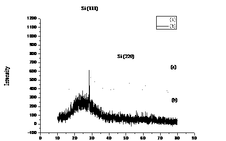
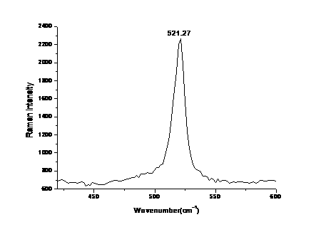
[0029] (3) The grown amorpho...


PUM

PropertyMeasurementUnit
Thicknessaaaaaaaaaa

Abstract

The invention relates to a method for inducing crystallization of an amorphous silicon thin film into a polycrystalline silicon thin film by aluminum at a low temperature, belonging to the technical field of preparation of the polycrystalline silicon thin film. By using the catalytic action of the metal aluminum, the amorphous silicon thin film is induced to be crystallized into the polycrystalline silicon thin film through a two-step annealing method at the low temperature so as to reduce the metal contamination. According to the main technical scheme provided by the invention, the method comprises the steps of: taking glass as a growth substrate and then preparing amorphous silicon, silicon dioxide and aluminum films in sequence to form a multiple-interface structure; then performing two-step annealing, i.e., performing rapid annealing, subsequently placing a sample in an annealing furnace to perform slow annealing, corroding to remove aluminum and drying with nitrogen; and finally, preparing the polycrystalline silicon thin film crystallized under the induction of the aluminum, wherein the grain size is about 50-200 nm. According to the method, the metal contamination in the metal induced crystallization (MIC) technology can be effectively relieved; and the method is suitable for preparing photoelectric devices such as a field effect transistor and a thin film solar cell.

Description

technical field [0001] The invention relates to a preparation method for inducing the crystallization of an amorphous silicon film into a polysilicon film at a low temperature by metal aluminum, which mainly utilizes the catalytic effect of metal aluminum to induce the crystallization of an amorphous silicon film into a polysilicon film at a low temperature, which belongs to polysilicon Thin film preparation technology field. Background technique [0002] At present, the methods for preparing polysilicon thin films mainly include: low pressure chemical vapor deposition (LPCVD), solid phase crystallization (SPC), excimer laser induced crystallization (ELA), rapid thermal annealing crystallization (RTA), etc. [0003] The polysilicon film prepared by LPCVD method is dense and uniform, and can be produced in a large area, but when prepared by this method, the required substrate temperature is high and the deposition speed is slow, and cheap glass cannot be used as the substrate...

Claims


Application Information

Patent Timeline
IPC IPC(8): H01L21/203H01L21/324
Inventor 史伟民钱隽金晶李季戎廖阳王国华许月阳
Owner SHANGHAI UNIV
Features
  • R&D
  • Intellectual Property
  • Life Sciences
  • Materials
  • Tech Scout
  • Unparalleled Data Quality
  • Higher Quality Content
  • 60% Fewer Hallucinations
Learn More