Fabrication method of anti-esd integrated soi LDMOS device unit

A manufacturing method and device technology, applied in semiconductor/solid-state device manufacturing, electrical components, circuits, etc., can solve the problems of increasing system volume, weight and cost, SOILDMOS devices without integrated anti-ESD structure and function, device failure, etc., to achieve Excellent electrical and thermal properties, excellent integrated anti-ESD self-protection effect

Active Publication Date: 2015-08-19
HANGZHOU DIANZI UNIV
View PDF5 Cites 0 Cited by
  • Summary
  • Abstract
  • Description
  • Claims
  • Application Information

AI Technical Summary

Problems solved by technology

[0012] These SOI LDMOS devices do not integrate anti-ESD structures and functions. Due to their inherent MOS (metal-oxide-semiconductor) structures, it is easy to cause high-voltage static electricity above kilovolts during packaging, transportation, assembly and use.
If there is no stable diode clamp protection, due to the thin gate oxide layer, it is easy to be broken down by this high voltage static electricity and cause permanent failure of the device
The permanent failure of the device caused by gate breakdown caused by high voltage static electricity is called electrostatic damage (ESD)
At present, commercialized SOI LDMOS devices need external discrete Zener diodes for protection, which increases system size, weight and cost, and reduces reliability.

Method used


Image

  • Fabrication method of anti-esd integrated soi LDMOS device unit
  • Fabrication method of anti-esd integrated soi LDMOS device unit

Examples


Embodiment Construction

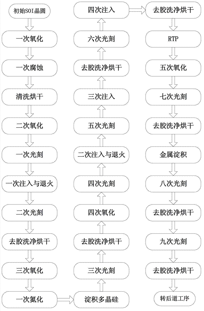
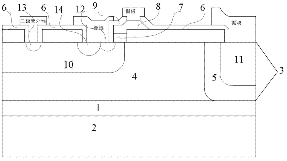
[0030] Such as figure 1 and figure 2 Shown, the fabrication method of anti-ESD integrated SOI LDMOS device unit comprises the following steps:

[0031] Step (1) select the silicon wafer of the first conductivity type, a buried insulating layer 1 is formed at a certain depth below the surface of one side of the silicon wafer, and the buried insulating layer 1 completely isolates the silicon wafer into two semiconductor regions, The thick one of the two semiconductor regions is used as the substrate 2, and the thin one has the second conductivity type and a certain doping concentration distribution, and is used as the top layer silicon film 3 for making devices and circuits; wherein, the top layer silicon film 3 is greater than 50 The area of ​​% is used as the drift zone 4 of making device;

[0032] The certain depth mentioned is determined according to the actual situation.

[0033] Step (2) Carry out the first oxidation on the upper surface of the exposed top layer silico...


PUM


Abstract

The invention relates to a manufacturing method of an anti-ESD integration SOI LDMOS device unit. By using the SOI LDMOS device manufactured through using the prior art, system weight is heavy; cost is high and reliability is low. According to the invention, through using five-time oxidation and nine-time photoetching, the SOI LDMOS device unit which integrates an anti-ESD structure and a function is manufactured. By using the method of the invention, under the condition that chip area cost is increased slightly, the integrated power and radio frequency SOI LDMOS device possesses an excellent integrated anti-ESD self-protection function; anti-ESD self-protection performance of the SOI LDMOS device is significantly improved; sizes, weight and cost of various kinds of power electronics systems using the device are reduced; and system reliability is increased.

Description

technical field [0001] The invention belongs to the technical field of semiconductors, and relates to a method for manufacturing an anti-ESD (electrostatic damage) integrated SOI (silicon on insulating layer) LDMOS (laterally diffused metal-oxide-semiconductor) device unit. Background technique [0002] SOI LDMOS devices are used as non-contact power electronic switches due to their small size and weight, high operating frequency, high operating temperature and strong radiation resistance, low cost and high reliability. , power driver or RF power amplifying transistor are widely used in technical fields such as intelligent power electronics, high temperature environment power electronics, space power electronics, vehicle power electronics, military and communication. SOI CMOS VLSI process technology has advantages such as high process maturity, good dielectric isolation performance, simple isolation process, easy three-dimensional integration, easy integration of micro-optic...

Claims


Application Information

Patent Timeline
Patent Type & Authority Patents(China)
IPC IPC(8): H01L21/336
Inventor 张海鹏余育新洪玲伟孟晓李俊杰朱仁根章红芳
Owner HANGZHOU DIANZI UNIV
Why Eureka
Try Eureka