Etching-based one-dimensional electron gas GaN-based HEMT (high electron mobility transistor) device and preparation method thereof

An electronic gas and device technology, applied in the field of microelectronics, can solve the problems of electron concentration limitation, small breakdown electric field, poor electron transport characteristics, etc., and achieve the effect of improving power characteristics, improving high temperature and high pressure characteristics, and good power characteristics

Active Publication Date: 2013-10-23
云南凝慧电子科技有限公司
View PDF2 Cites 4 Cited by
  • Summary
  • Abstract
  • Description
  • Claims
  • Application Information

AI Technical Summary

Problems solved by technology

However, due to the poor material properties of Si and GaAs semiconductors, the one-dimensional electron gas characteristics are far below ideal
First of all, due to the small bandgap width of Si and GaAs semiconductor materials, the intrinsic carrier concentration is high and the breakdown electric field is small, which makes the prepared Si-based and GaAs-based devices have poor high-temperature and high-voltage characteristics and poor radiation re

Method used


Image

  • Etching-based one-dimensional electron gas GaN-based HEMT (high electron mobility transistor) device and preparation method thereof
  • Etching-based one-dimensional electron gas GaN-based HEMT (high electron mobility transistor) device and preparation method thereof
  • Etching-based one-dimensional electron gas GaN-based HEMT (high electron mobility transistor) device and preparation method thereof

Examples


Embodiment 1

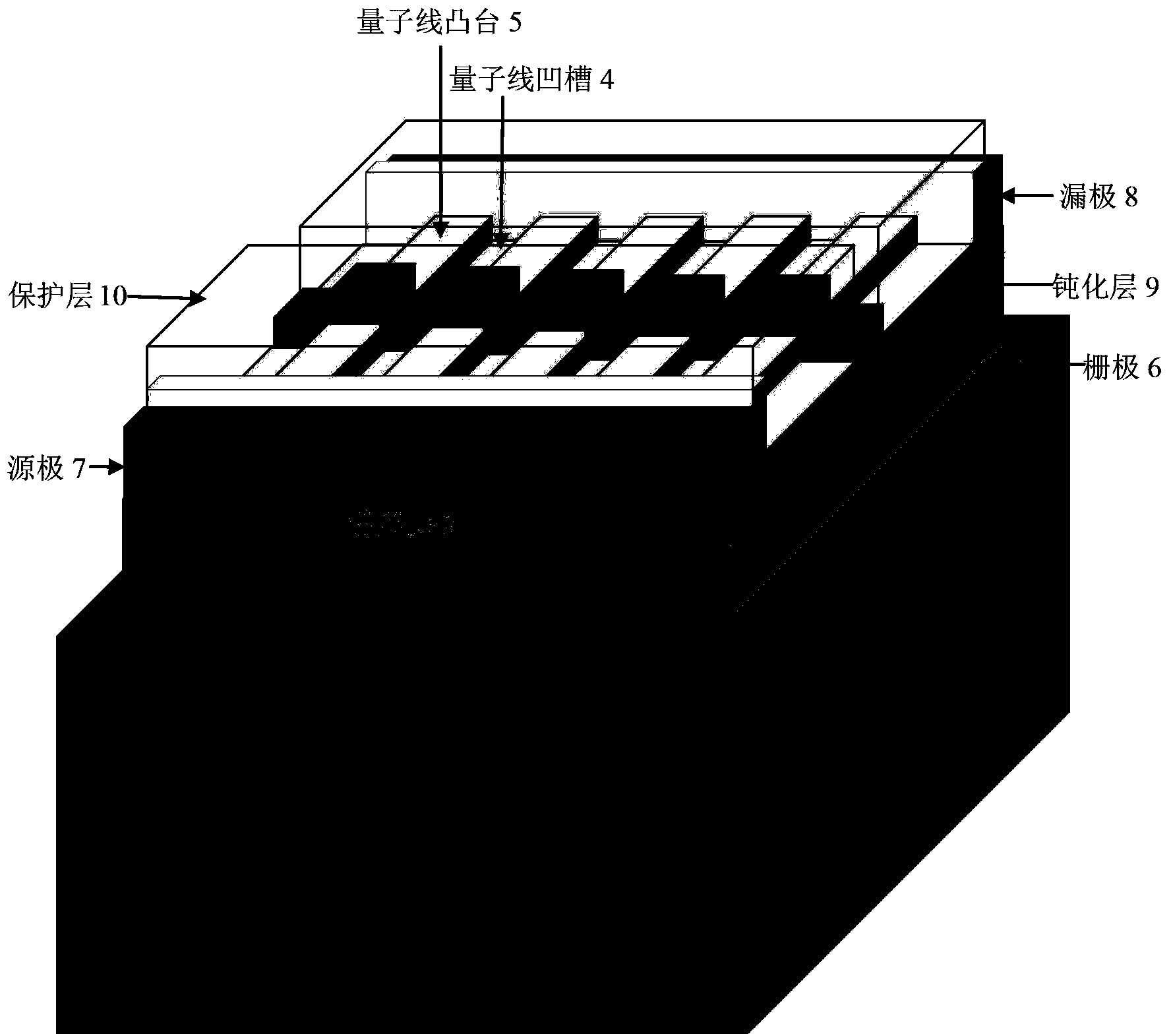
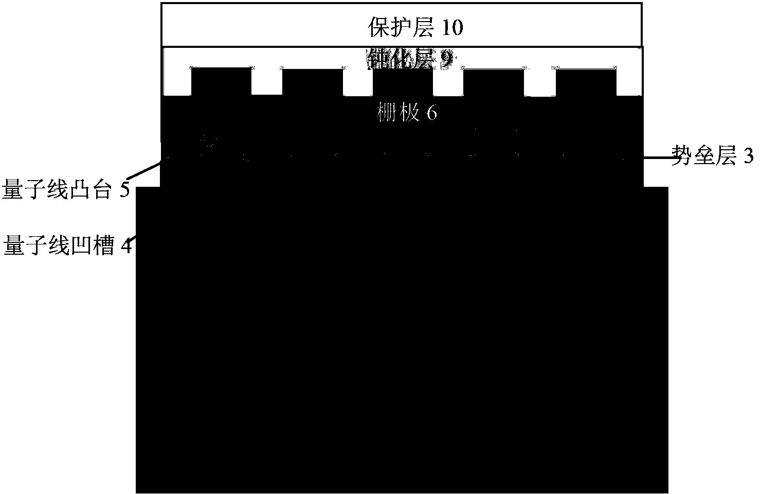
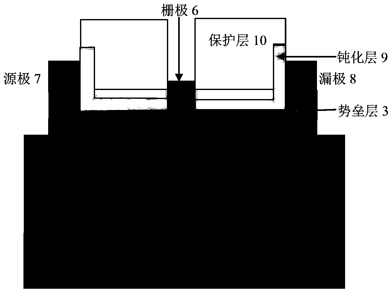
[0051] Embodiment 1, the production substrate 1 is sapphire, the buffer layer 2 is GaN, the barrier layer 3 is AlGaN, the passivation layer 9 is SiN, the protective layer 10 is SiN, the depth of the quantum wire groove 4 is 8nm, and the width is 50nm. A one-dimensional electron gas GaN-based HEMT with a width of 10 nm of quantum wire bosses 5 and a periodic arrangement of quantum wire grooves 4 and quantum wire bosses 5 .

[0052] Step 1, using MOCVD to epitaxially GaN semiconductor material with a thickness of 1 μm on the sapphire substrate 1 as the buffer layer 2; the process conditions for the epitaxial GaN buffer layer 2 are: the temperature is 1000°C, and the pressure is 200 Torr , the hydrogen flow rate is 4800 sccm, the ammonia gas flow rate is 4800 sccm, and the gallium source flow rate is 200 μmol / min.

[0053] Step 2: Deposit an AlGaN semiconductor material with a thickness of 10 nm on the buffer layer 2 by MOCVD as a barrier layer 3, and the Al composition of the Al...

Embodiment 2

[0070] Embodiment 2, the production substrate 1 is silicon carbide, the buffer layer 2 is GaN, the barrier layer 3 is AlGaN, the passivation layer 9 is SiN, and the protective layer 10 is SiO 2 , the quantum wire groove 4 has a depth of 28nm, a width of 250nm, a quantum wire boss 5 width of 50nm, and a one-dimensional electron gas GaN-based HEMT in which the quantum wire groove 4 and the quantum wire boss 5 are arranged periodically.

[0071] Step 1, epitaxially epitaxially GaN buffer layer 2 with a thickness of 3 μm on silicon carbide substrate 1 .

[0072] Using metal organic chemical vapor deposition MOCVD equipment under the process conditions of temperature 1020 ° C, pressure 200 Torr, hydrogen flow rate 5000 sccm, ammonia gas flow rate 5000 sccm, gallium source flow rate 220 μmol / min, epitaxy on silicon carbide substrate 1 GaN buffer layer 2 with a thickness of 3 μm.

[0073] Step 2, depositing an AlGaN barrier layer 3 with a thickness of 30 nm on the GaN buffer layer 2...

Embodiment 3

[0097] Embodiment 3, the production substrate 1 is silicon, the buffer layer 2 is GaN, the barrier layer 3 is AlGaN, and the passivation layer 9 is SiO 2 , the protective layer 10 is SiN, the depth of the quantum wire groove 4 is 48nm, the width is 500nm, the width of the quantum wire boss 5 is 100nm, and the one-dimensional electron gas GaN of the quantum wire groove 4 and the quantum wire boss 5 are arranged periodically Base HEMT.

[0098] In step A, a GaN buffer layer 2 with a thickness of 5 μm is epitaxially formed on the silicon substrate 1 .

[0099] A GaN buffer layer 2 with a thickness of 5 μm was epitaxially grown on a silicon substrate 1 using metal-organic chemical vapor deposition MOCVD equipment; The gas flow rate is 5200 sccm, and the gallium source flow rate is 240 μmol / min.

[0100] Step B, depositing an AlGaN barrier layer 3 with a thickness of 50 nm on the GaN buffer layer 2 .

[0101] Metal-organic chemical vapor deposition MOCVD equipment is used to dep...


PUM

PropertyMeasurementUnit
Thicknessaaaaaaaaaa
Widthaaaaaaaaaa
Widthaaaaaaaaaa

Abstract

The invention discloses an etching-based one-dimensional electron gas GaN-based HEMT (high electron mobility transistor) device and preparation method thereof, and mainly solves the problems that the conventional one-dimensional electron gas device has low high-temperature and high-pressure characteristics, frequency characteristics and power characteristics. The device comprises a substrate, a buffering layer, a potential barrier layer, a passivation layer and a protection layer from top to bottom; the two ends of the potential barrier layer are respectively a source and a drain; the passivation layer is positioned on the potential barrier layer between the source and the drain; a gate groove is formed in the passivation layer; and a gate is arranged in the gate groove. A plurality of quantum wire grooves which are arranged uniformly are etched on the potential barrier layer so as to obtain a plurality of quantum wire bosses with the width of nanoscale; and one-dimensional electron gas is formed in heterogenous junctions of the quantum wire bosses. The buffering layer adopts GaN; and the potential barrier layer adopts AlGaN. Compared with a Si-based device and a GaAs-based device, the etching-based one-dimensional electron gas GaN-based HEMT device has high high-temperature and high-pressure characteristics, frequency characteristics and power characteristics, and can be used for manufacturing ultrahigh speed low-power consumption one-dimensional electron gas devices.

Description

technical field [0001] The invention belongs to the technical field of microelectronics and relates to a semiconductor device, in particular a one-dimensional electron gas HEMT device based on a GaN semiconductor material heterojunction structure, which can be used as a basic device of a microwave, millimeter wave communication system and a radar system. Background technique [0002] III-V compound semiconductor materials are the third-generation semiconductor materials that have been developed rapidly for more than ten years, such as GaN-based, GaAs-based, InP-based and other semiconductor materials, which have a large band gap and can be combined with InN, AlN, etc. Alloy semiconductors are formed to make their forbidden band width adjustable. People usually use these III-V compound semiconductor materials to form various heterojunction structures. Due to the large difference in the forbidden band width of the III-V compound semiconductor materials on both sides of the het...

Claims


Application Information

Patent Timeline
IPC IPC(8): H01L29/778H01L29/06H01L21/335
Inventor 马晓华陈伟伟汤国平郝跃赵胜雷
Owner 云南凝慧电子科技有限公司
Why Eureka
Try Eureka