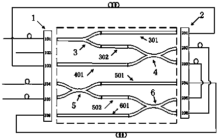
Cascaded Mach-Zehnder interferometer based reconfigurable comb filter and preparation method thereof
A comb filter and interferometer technology, applied in the direction of instruments, light guides, optics, etc., can solve the problems of optical path difference, fixed output characteristics, unfavorable light sensing, etc., and achieve high thermal stability, low nonlinearity, The effect of low loss
- Summary
- Abstract
- Description
- Claims
- Application Information
AI Technical Summary
Problems solved by technology
Method used
Image
Examples
preparation example Construction
[0040] The method for preparing a reconfigurable comb filter based on the cascaded Mach-Zehnder interferometer includes the following steps:
[0041] Step 10): Take a silicon substrate and clean the silicon wafer by wet chemical method. A silicon dioxide buffer layer with a thickness of 15 μm to 20 μm is prepared on the silicon substrate by the thermal oxidation method. Using plasma enhanced chemical vapor deposition method, the concentration of silane and nitrogen is 5% S i H 4 :N 2 , Temperature 250℃-400℃, doping germanium dioxide in silicon dioxide to obtain a waveguide layer 9 with a thickness of 8μm, using GeH with a gas concentration of 10% 4 :Ar, forming a waveguide layer with a thickness of 8μm, and the refractive index of the waveguide layer is higher than that of the silica buffer layer by 0.4%.
[0042] Step 20): On the waveguide layer, using photolithography and etching processes, prepare the PLC chip part based on the cascaded Mach-Zehnder interferometer type reconfigu...
Embodiment
[0051] The following describes the preparation method of the reconfigurable comb filter based on the cascaded Mach-Zehnder interferometer, so as to give a more detailed description of the above preparation method.
[0052] Step 10): Fabricate the silicon dioxide buffer layer 8 and the waveguide 9. Reference figure 2 As shown, it includes step 101), step 102) and step 103).
[0053] Step 101) Take a silicon substrate, clean the silicon wafer or substrate 7 with a wet chemical method to remove the dirt on the surface; then, after ultrasonic cleaning and drying of deionized water ultrasonic waves, the cleaning of the silicon wafer is completed;
[0054] Step 102) Prepare the silicon dioxide buffer layer 8. There are many methods for preparing the silicon dioxide buffer layer 8, such as chemical vapor deposition (CVD), flame hydrolysis (FHD), sol-gel method (Sol-Gel), Thermal oxidation method (TO) etc. Since the thermal oxidation method can oxidize more than 100 silicon wafers at the ...
PUM
| Property | Measurement | Unit |
|---|---|---|
| Thickness | aaaaa | aaaaa |
| Thickness | aaaaa | aaaaa |
Abstract
Description
Claims
Application Information


