
Optical amplifier device

一种光放大、信号光的技术,应用在激光器、激光器零部件、光学等方向,能够解决传输品质下降、信号光降低3dB、传输误码率上升等问题

Active Publication Date: 2013-11-20
NIPPON TELEGRAPH & TELEPHONE CORP
View PDF0 Cites 6 Cited by
  • Summary
  • Abstract
  • Description
  • Claims
  • Application Information

AI Technical Summary

Problems solved by technology

However, these laser amplifiers cannot shape the degraded signal light pulse waveform
In addition, since natural radiation that has nothing to do with signal components is mixed into these laser amplifiers, and this natural radiation is inevitable and occurs randomly, the S / N ratio of signal light is reduced by at least 3dB before and after amplification
This will lead to an increase in the transmission bit error rate during digital signal transmission and a decrease in transmission quality

Method used


Image

  • Optical amplifier device
  • Optical amplifier device
  • Optical amplifier device

Examples


no. 1 approach )

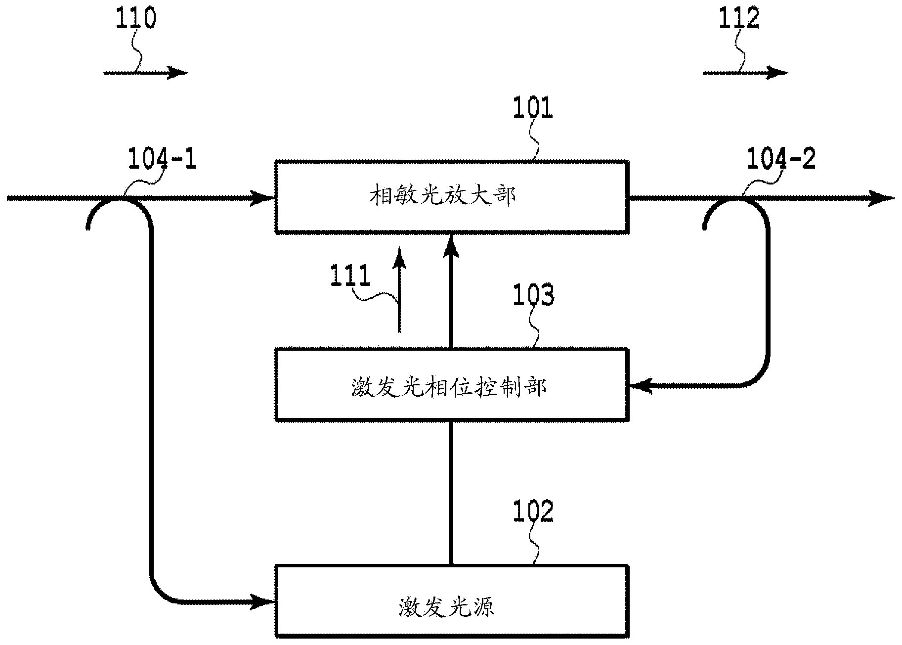
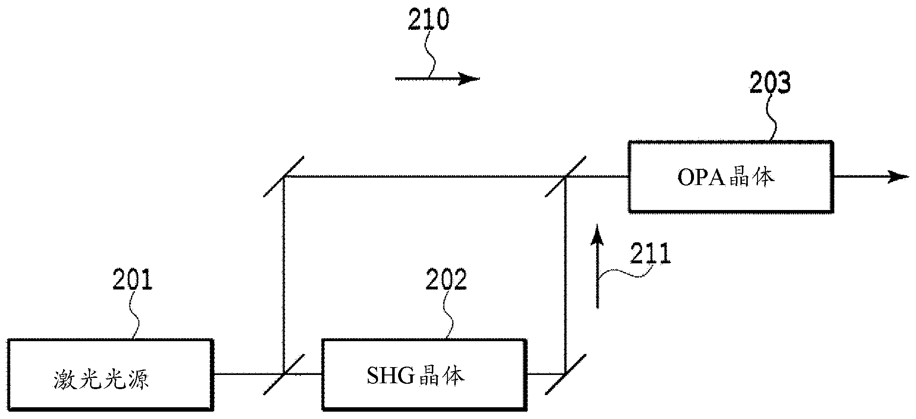
[0159] Figure 6 The structure of this embodiment is shown. In the present embodiment, the fundamental wave light 621 is amplified using a fiber laser amplifier (EDFA) 601 in order to obtain sufficient power for obtaining nonlinear optical effects from weak laser light used in optical communication. The amplified fundamental wave light 621 is incident to the first quadratic nonlinear optical element 602 - 1 to generate a second harmonic wave 622 . The phase-sensitive amplification is performed by performing degenerate parametric amplification on the incident signal light 620 and the second harmonic wave 622 to the second quadratic nonlinear optical element 602 - 2 . The structure of the phase-sensitive optical amplifying device is an essential feature of the present invention.

[0160] Figure 6 The shown structure will be described in detail later, and if such a structure is adopted, effects that cannot be obtained by the following prior art can be obtained.

[0161] Fi...

no. 2 approach )

[0179] Figure 9 The structure of this embodiment is shown. By utilizing the waveform shaping effect of the phase-sensitive optical amplifier of the present invention, it is possible to remove the chirp when sending a signal even if a modulator with chirp is used. After the output from the external resonant semiconductor LD (ECL) 930 is NRZ intensity modulated at a modulation speed of 40Gb / s using an electric field absorption (EA) modulator, it passes through a phase-sensitive optical amplifier similar to that of the first embodiment To amplify the modulated signal, thus forming a transmitter.

[0180] Electric field absorption (EA) modulators can be produced cheaply and in large quantities because they can be fabricated using semiconductors. However, since frequency chirp components are superimposed in the modulated signal by electric field absorption, the signal quality is degraded. That is, the output phase of the modulator fluctuates when transitioning between ON and OF...

no. 3 approach )

[0188] Figure 12 The structure of this embodiment is shown. The data-modulated signal light 1240 propagates through a transmission medium such as an optical fiber, and the signal is transmitted. Figure 12 In this case, a configuration is shown in which an in-phase optical amplifier is used as a relay amplifier that performs optical amplification to compensate for loss of light intensity in a transmission medium.

[0189] When the light source for generating signal light is arranged near the phase-sensitive light amplifier, part of the light source for signal light can be branched as fundamental wave light. However, when a phase-sensitive optical amplifier is used as a relay amplifier in optical transmission, it is necessary to synchronize the phases of the fundamental light and the signal light in the phase-sensitive optical amplifier device using, for example, a phase synchronization device as described below.

[0190] In this embodiment, as the input signal light, an opt...


PUM

PropertyMeasurementUnit
wavelengthaaaaaaaaaa

Abstract

The purpose of the present invention is to provide a phase-sensitive optical amplifier device, which can be adapted for optical communication and can provide low noise amplification. A phase-sensitive optical amplifier device according to the present invention is a phase-sensitive optical amplifier device, which amplifies signal light by optical mixing using nonlinear optical effect, comprising a first second-order nonlinear optical element (602-1) and a second second-order nonlinear optical element (602-2). The first second-order nonlinear optical element (602-1) generates from fundamental wave light (621) second harmonic light (622) used as excitation light and is provided with a filter (606-1) that separates only the second harmonic light from the fundamental wave light and the second harmonic light. The second second-order nonlinear optical element (602-2) is provided with a multiplexer (606-2) that mixes the signal light and the second harmonic light, performs parametric amplification using the multiplexed signal light and second harmonic light, and is provided with a filter (606-3) that separates only the amplified signal light from the second harmonic light and the amplified signal light.

Description

technical field [0001] The present invention relates to an optical amplifier device, and more particularly, to an optical amplifier device used in an optical communication system and an optical measurement system, and an optical transmitting device and an optical receiving device equipped with the optical amplifier device. Background technique [0002] In the existing optical transmission system, in order to regenerate the attenuated signal due to propagation in the optical fiber, the optical signal is converted into an electrical signal by using an identification and regeneration optical repeater, and then the optical signal is regenerated after identifying the digital signal. However, this identification and regenerative optical repeater has problems such as a limited response speed of electronic components that convert optical signals into electrical signals, or increased power consumption if the transmission speed of signals is high. [0003] As an amplification device t...

Claims


Application Information

Patent Timeline
Patent Type & Authority Applications(China)
IPC IPC(8): G02F1/39G02F1/37
CPCH01S3/0092G02F1/3544G02F1/3532G02F2001/392G02F1/37H01S3/2391G02F1/3534G02F1/39G02F1/3536G02F1/392H01S3/06754H01S3/1083
Inventor 游部雅生梅木毅伺圆佛晃次登仓明雄宫本裕高良秀彦竹之内弘和富田勲
Owner NIPPON TELEGRAPH & TELEPHONE CORP
Learn More