Silicone substrate high-linearity low-phase-shift ultra-broad-band digital attenuator

A digital attenuator, high linearity technology, applied in the electronic field, can solve the problems of increasing the manufacturing cost of the attenuator, poor linearity, large chip area, etc., achieve good port matching characteristics, low signal power loss, and realize single chip Effect

Active Publication Date: 2013-12-04
XIDIAN UNIV
View PDF5 Cites 25 Cited by
  • Summary
  • Abstract
  • Description
  • Claims
  • Application Information

AI Technical Summary

Problems solved by technology

The disadvantage of the attenuation module disclosed in this patented technology is that the electronically controlled attenuator module is used as the PIN diode of the control switch in this patented technology, which cannot be directly processed and manufactured by the existing silicon-based CMOS or BiCMOS process, and additional process steps are required manufacturing, which increases the manufacturing cost of the attenuator
Although the numerically controlled attenuator disclosed in this patent application document has low insertion loss and additional phase shift, there are still shortcomings: the high electron mobility transistor of the gallium arsenide process is used in the numerically controlled attenuator as the state of the different attenuation modules Switching control switch, high production cost, low yield
Although it has the adv

Method used


Image

  • Silicone substrate high-linearity low-phase-shift ultra-broad-band digital attenuator
  • Silicone substrate high-linearity low-phase-shift ultra-broad-band digital attenuator
  • Silicone substrate high-linearity low-phase-shift ultra-broad-band digital attenuator

Examples


Embodiment 1

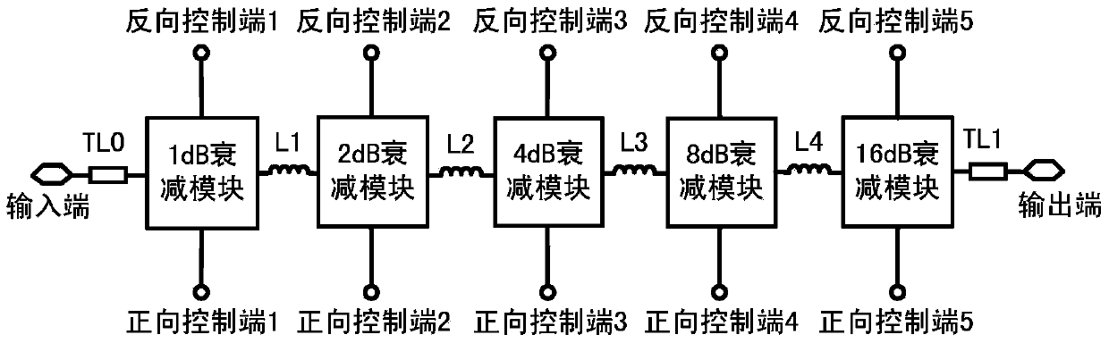
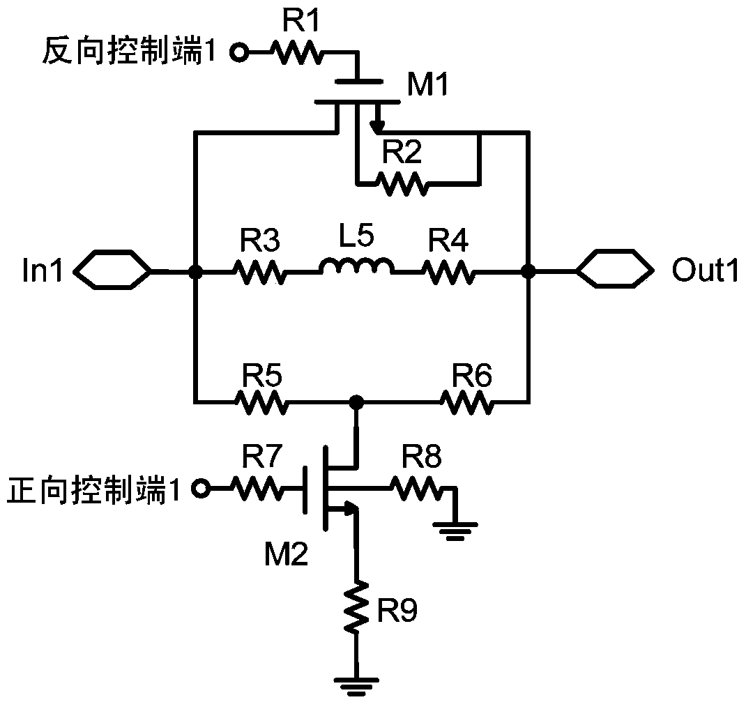
[0042] Embodiment 1: The working process of the 1dB attenuation module of the present invention.

[0043] Refer to attached figure 1 , attached figure 2 , Embodiment 1 of the present invention adopts a bridge T-shaped attenuation network structure to attach Figure 7 The shown NMOS transistor switch with channel parallel resistance structure is used as the control switch of the series branch, with the attached Figure 8 The shown bulk-suspended structure NMOS transistor switch is used as the control switch of the parallel branch, and the inductance compensation network is used for phase shift compensation. The 1dB attenuation module is controlled by a set of complementary digital signals at the forward control terminal 1 and the reverse control terminal 1 at the same time. When the forward control terminal 1 is at low level and the reverse control terminal 1 is at high level, the NMOS transistor M1 is turned on, the NMOS transistor M2 is turned off, and the 1dB attenuation...

Embodiment 2

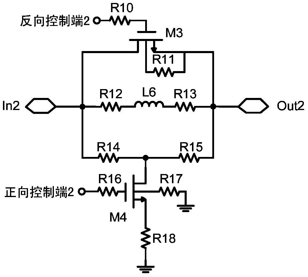
[0044] Embodiment 2: the working process of the 2dB attenuation module of the present invention.

[0045] Refer to attached figure 1 , attached image 3 , Embodiment 2 of the present invention adopts a bridge T-shaped attenuation network structure, with Figure 7 The shown NMOS transistor switch with channel parallel resistance structure is used as the control switch of the series branch, with the attached Figure 8 The shown bulk-suspended structure NMOS transistor switch is used as the control switch of the parallel branch, and the inductance compensation network is used for phase shift compensation. The 2dB attenuation module is controlled by a set of complementary digital signals at the forward control terminal 2 and the reverse control terminal 2 at the same time. When the forward control terminal 2 is at low level and the reverse control terminal 2 is at high level, the NMOS transistor M3 is turned on, the NMOS transistor M4 is turned off, and the 2dB attenuation modu...

Embodiment 3

[0046] Embodiment 3: the working process of the 4dB attenuation module of the present invention.

[0047] Refer to attached figure 1 , attached Figure 4 , Embodiment 3 of the present invention adopts bridge T-type attenuation network structure, with Figure 7 The shown NMOS transistor switch with channel parallel resistance structure is used as the control switch of the series branch, with the attached Figure 8 The NMOS transistor switch of the bulk suspension structure shown is used as the control switch of the parallel branch, and the phase shift compensation is performed by the capacitor compensation network. The 4dB attenuation module is controlled by a set of complementary digital signals at the forward control terminal 3 and the reverse control terminal 3 at the same time. When the forward control terminal 3 is at low level and the reverse control terminal 3 is at high level, the NMOS transistor M5 is turned on, the NMOS transistor M6 is turned off, and the 4dB atte...


PUM


Abstract

The invention discloses a silicone substrate high-linearity low-phase-shift ultra-broad-band digital attenuator which comprises a 1dB attenuating module, a 2dB attenuating module, a 4dB attenuating module, a 8dB attenuating module and a 16dB attenuating module. Two NMOS field effect transistors which are of a channel parallel-connection resistor structure and of a solid suspension structure and manufactured through SiGe BiCMOS technology are adopted to be used as control switches, five sets of complementary digital signals are used for controlling the five attenuating modules independently to work, a low-pass network is used for conducting phase compensation, inductance is used for matching between the adjacent attenuating modules, matching between the input end of the1dB attenuating module and 50 omega input impedance and matching between the output end of the 16dB attenuating module and 50 omega output impedance are realized through transmission wires, the working frequency range is 1-25GHz, and low-differential-loss low-phase-shift attenuation of signal amplitudes under 32 states can be realized with the 1dB length stepping in the attenuating range of 0-31dB. The silicone substrate high-linearity low-phase-shift ultra-broad-band digital attenuator has the advantages of being low in differential loss, low in accessory phase shift, high in linearity, low in production cost and low in chip area, and can be used for large-amplitude signal processing and single chip integration.

Description

technical field [0001] The invention belongs to the field of electronic technology, and further relates to a silicon-based high-linearity low-phase-shift ultra-wideband digital attenuator in the technical field of communication and radar system electronic components. The invention can be used in ultra-wideband communication systems, automatic gain control systems, phased array systems, electronic countermeasures systems, and CDMA communication systems to realize low-phase-shift gain change attenuation high linearity functional modules for signal amplitudes. Background technique [0002] At present, in the field of electronic components of communication and radar systems, ultra-wideband digital attenuators are widely used in ultra-wideband communication systems, automatic gain control systems, phased array systems, electronic countermeasure systems, and CDMA communication systems. The digital attenuator with precise attenuation accuracy and high linearity enables communicatio...

Claims


Application Information

Patent Timeline
IPC IPC(8): H03H7/24
Inventor 庄奕琪李振荣张岩龙靳刚汤华莲张丽李聪曾志斌
Owner XIDIAN UNIV
Why Eureka
Try Eureka