Method for preparing Ge component and bandwidth regulated SiGe nanobelt

A nanobelt and bandwidth technology, applied in the field of preparation of SiGe nanobelts, can solve the problems of uneven nanowires, metal catalysis pollution, Ge component regulation, etc., and achieve the effects of mature technology, accelerated speed and low cost.

Active Publication Date: 2013-12-11
XIAMEN UNIV
View PDF4 Cites 5 Cited by
  • Summary
  • Abstract
  • Description
  • Claims
  • Application Information

AI Technical Summary

Problems solved by technology

[0005] The purpose of the present invention is to provide a SiGe nanometer with adjustable Ge composition and bandwidth for the problems of metal catalytic pollution, uneven nanowire, limited length, and control of Ge composition in the current preparation method of semiconductor nanowires. Belt preparation method

Method used


Image

  • Method for preparing Ge component and bandwidth regulated SiGe nanobelt
  • Method for preparing Ge component and bandwidth regulated SiGe nanobelt
  • Method for preparing Ge component and bandwidth regulated SiGe nanobelt

Examples


Embodiment Construction

[0020] The following embodiments will further illustrate the present invention in conjunction with the accompanying drawings.

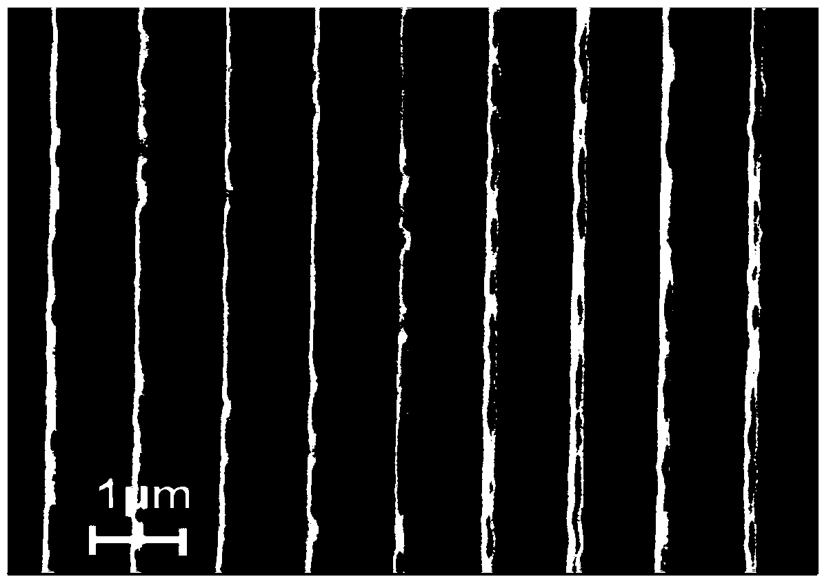
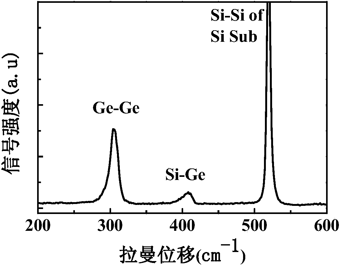
[0021] figure 1 A schematic flow chart of preparing SiGe nanoribbons with adjustable Ge composition and bandwidth is given in the present invention. Among them: 1 is silicon substrate, 2 is SiO 2 layer, 3 is the silicon-on-insulator layer; 4 is the Si / SiGe / Si structure epitaxially grown by the ultra-high vacuum chemical vapor deposition system; 5 is the photoresist; 6 is the SiO formed by oxidation 2 Layer; 7 is the SiGe nanoribbon with high Ge composition generated by oxidation and concentration.

[0022] Epitaxially grow Si / SiGe / Si structures on SOI substrates; perform standard cleaning of silicon wafers on the samples, and coat a photoresist with a thickness of about 500nm; then use holographic laser interference to perform photolithography to obtain a grating array with a period of less than 1 μm; then Etching of SiO to buried layer by combinat...


PUM


Abstract

The invention discloses a method for a preparing Ge component and bandwidth regulated SiGe nanobelt and relates to a nano-material. The method comprises the following steps: generating a Si/SiGe/Si structure on an SOI substrate by using a molecular beam epitaxy method or a chemical vapor deposition method; performing exposing and developing on an obtained sample by using holographic laser interferometry, obtaining an optical grating array with a period below 1 [mu] m, etching a pattern by using an ICP dry method and a wet method, and etching a buried layer SiO2 layer with a depth reaching the SOI substrate; and performing selective oxidation and annealing on the sample by using a conventional resistor type heating oxidation furnace, and obtaining the Ge component and bandwidth regulated SiGe nanobelt with a bandwidth reaching below 200 nm. According to the Ge component and bandwidth regulated SiGe nanobelt, the epitaxial Si and SiGe on the SOI substrate are oxidated through a local selective oxidation mode, so that the bandwidth is reduced, Ge components are regulated for preparing and generating a semiconductor material with nanometer scale, and the method is simple, low-cost, and compatible with a silicon conventional process.

Description

technical field [0001] The invention relates to a nanometer material, in particular to a preparation method of a SiGe nanobelt whose Ge composition and bandwidth can be adjusted. Background technique [0002] As a new type of material, nanomaterials have shown good application prospects. At present, the research hotspots on the application of nanomaterials mainly focus on nanotubes, nanowires, nanofilms, and nanocomposites. With the reduction of device size, physical effects such as quantum confinement effect and Coulomb blockade effect will become more and more significant, which will reveal new properties of nano-semiconductor materials from a deeper level and lay a foundation for the application of nano-devices. Although some functions of nano-devices such as nano-transistors and sensors have been preliminarily realized, the research on nano-devices is still in the initial stage, and there is still a considerable distance from the large-scale integration of nano-devices. ...

Claims


Application Information

Patent Timeline
Patent Type & Authority Applications(China)
IPC IPC(8): H01L21/02H01L21/20B82Y40/00
Inventor 李成卢卫芳黄诗浩林光杨陈松岩
Owner XIAMEN UNIV
Why Eureka
Try Eureka