Self-driven full-bridge synchronous rectification circuit
A synchronous rectification and self-driving technology, applied in electrical components, output power conversion devices, conversion of AC power input into DC power output, etc. Bridge rectification loss, the effect of simplifying the circuit structure
- Summary
- Abstract
- Description
- Claims
- Application Information
AI Technical Summary
Problems solved by technology
Method used
Image


Examples
Embodiment 1
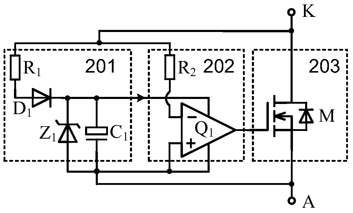
[0042] refer to figure 2 with Figure 4, each self-driven active switch includes a power supply circuit, a drive circuit and an execution circuit, wherein the power supply circuit includes a current limiting resistor RA, a switching diode DA, a voltage regulator tube Z, and an energy storage capacitor C; the drive circuit includes a protection resistor RB and an operation circuit Amplifier Q; the execution circuit includes an N-channel MOSFET M with a parasitic diode DB;
[0043] The current-limiting resistor RA is connected between the anode of the switching diode DA and the drain D of the N-channel MOSFET M, the energy storage capacitor C is connected in parallel to the regulator Z, and the anode of the regulator Z is connected to the N The source S of the channel MOSFET tube M, and the negative pole of the voltage regulator tube are connected to the negative pole of the switching diode D;
[0044] In the operational amplifier Q, its inverting input terminal is connected ...
Embodiment 2
[0059] refer to image 3 with Figure 5 , the self-driven active switch of the present invention includes a power supply circuit, a drive circuit and an execution circuit, wherein
[0060] The power supply circuit includes a current-limiting resistor RA, a switching diode DA, a voltage regulator tube Z, and an energy storage capacitor C; the drive circuit includes a protection resistor RB and an operational amplifier Q; the execution circuit includes a P-channel MOSFET tube with a parasitic diode DB;
[0061] The first resistor RA is connected between the cathode of the switching diode DA and the drain D of the P-channel MOSFET, the energy storage capacitor C is associated with the voltage regulator transistor Z, and the cathode of the voltage regulator transistor Z is connected to the P-channel The source S of the MOSFET tube, the anode of the Zener tube is connected to the anode of the switching diode DA;
[0062] Described operational amplifier Q, its inverting input term...
PUM
 Abstract
Description
Claims
Application Information