Nitrogen polar surface light emitting diode with tunnel junction structure

A technology of tunnel junction and nitrogen polarity, used in electrical components, circuits, semiconductor devices, etc., can solve problems that are not very obvious in practice, and achieve the effect of improving ohmic contact and current expansion capabilities

Active Publication Date: 2014-01-01
SOUTHEAST UNIV
View PDF2 Cites 19 Cited by
  • Summary
  • Abstract
  • Description
  • Claims
  • Application Information

AI Technical Summary

Problems solved by technology

In addition, the effect of only using the n+-GaN layer as an ohmic contact between the topmost s

Method used


Image

  • Nitrogen polar surface light emitting diode with tunnel junction structure
  • Nitrogen polar surface light emitting diode with tunnel junction structure

Examples


Embodiment Construction

[0022] The present invention will be further described below in conjunction with the accompanying drawings.

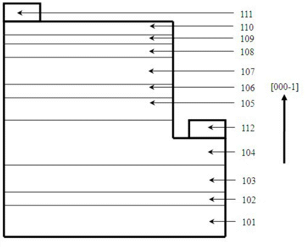
[0023] Such as figure 1 Shown is a nitrogen polar surface LED chip grown along the [000-1] direction, with a p-i-n tunnel junction structure as the top ohmic contact layer, including a sapphire substrate 101 and a low-temperature nucleation layer 102 arranged in sequence from bottom to top , non-doped semiconductor layer 103, n-type semiconductor layer 104, multi-quantum well active layer 105, p-AlGaN electron blocking layer 106, p-type semiconductor layer 107, p + -GaN layer 108, undoped In x Al y Ga 1-x-y N layer 109 , n-type superlattice structure layer 110 and metal electrode 111 .

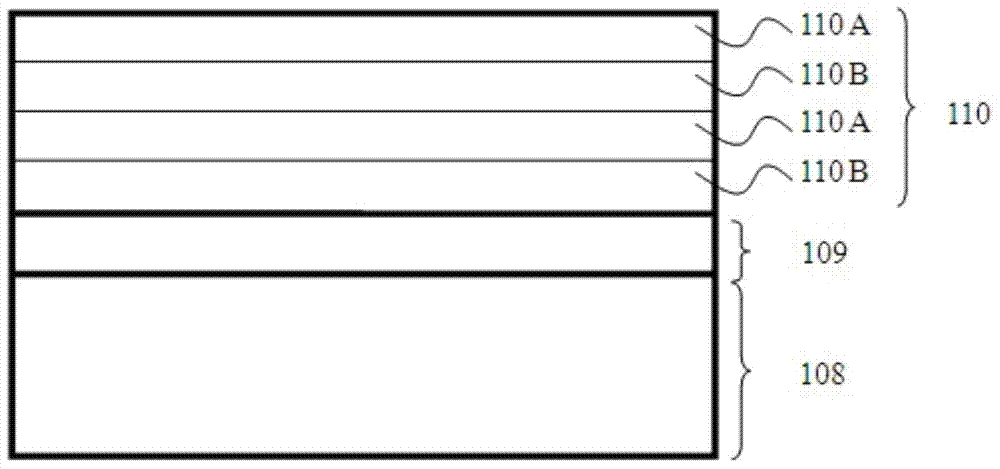
[0024] the p + -GaN layer 108, undoped In x Al y Ga 1-x-y The N layer 109 and the n-type superlattice structure layer 110 together form a p-i-n tunnel junction structure. Such as figure 2 Shown is the p-i-n tunnel junction structure of this example, and the n-type superlatti...


PUM

PropertyMeasurementUnit
Thicknessaaaaaaaaaa
Thicknessaaaaaaaaaa

Abstract

The invention discloses a nitrogen polar surface light emitting diode with a tunnel junction structure. The nitrogen polar surface light emitting diode with the tunnel junction structure comprises a sapphire substrate, a low temperature nucleating layer, a non-doped semiconductor layer, an n-type semiconductor layer, a multiple quantum well active layer, a p-AlGaN electronic barrier layer, a p-type semiconductor layer, a p+-GaN layer, a non-doped InxAlyGal-x-yN layer, an n-type superlattice layer and a metal electrode, wherein the sapphire substrate, the low temperature nucleating layer, the non-doped semiconductor layer, the n-type semiconductor layer, the multiple quantum well active layer, the p-AlGaN electronic barrier layer, the p-type semiconductor layer, the p+-GaN layer, the non-doped InxAlyGal-x-yN layer, the n-type superlattice layer and the metal electrode are arranged from bottom to top in sequence. The p+-GaN layer, the non-doped InxAlyGal-x-yN layer and the n-type superlattice layer form the p-i-n tunnel junction structure together. According to the nitrogen polar surface light emitting diode with the tunnel junction structure, the p-i-n tunnel junction structure is used as an ohmic contact layer on the top of an LED chip so that the current expanding capacity of an LED device can be improved, therefore, the turn-on voltage of the whole chip is reduced, and the light output power of the chip can be effectively improved.

Description

technical field [0001] The invention relates to a nitrogen polar surface light-emitting diode with a p-i-n tunnel junction as an ohmic contact layer structure on the top of an LED chip, which belongs to the manufacturing technology of semiconductor optoelectronic materials and devices. Background technique [0002] As a new type of high-efficiency solid-state light source, LED has significant advantages such as energy saving, environmental protection, long life, small size, and low operating voltage, and has been widely used in the world. [0003] In the existing LEDs made of III-V compound semiconductor materials, the III-V compound semiconductor materials are all grown along the [0001] direction, that is, the C-plane direction, and finally GaN, Ni Aluminum and their alloy crystals. In existing LEDs, p-type AlGaN / GaN and p-type InGaN / GaN have been widely used as the ohmic contact layer between the p-terminal and the metal electrode, so as to obtain a lower ohmic contact re...

Claims


Application Information

Patent Timeline
IPC IPC(8): H01L33/06
CPCH01L33/14
Inventor 张雄杨旭崔一平
Owner SOUTHEAST UNIV
Why Eureka
Try Eureka