Pressure sensor based on micro-structure gate insulation layer and manufacturing method thereof
A technology of pressure sensor and gate insulating layer, which is applied in the field of pressure sensor based on microstructured gate insulating layer and its preparation, can solve the problems of poor sensor uniformity, unfavorable preparation, large difference, etc., and achieve the effect of high sensitivity
- Summary
- Abstract
- Description
- Claims
- Application Information
AI Technical Summary
Problems solved by technology
Method used
Image

Examples
preparation example Construction
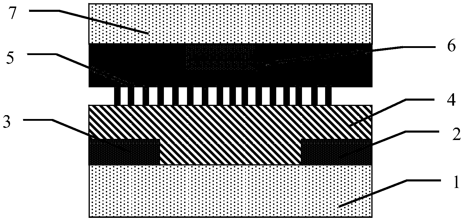
[0026] In addition, the present invention also provides a method for preparing a pressure sensor based on a microstructured gate insulating layer, comprising the following steps:
[0027] S1. Prepare a source electrode 2 and a drain electrode 3 on the substrate 1;
[0028] S2, on the source electrode 2, the drain electrode 3 and the substrate 1, prepare cross-linked semiconductor nanocrystals as the active layer 4;
[0029] S3. On the flexible substrate 7, prepare the gate electrode 6;
[0030] S4, preparing an insulating layer on the flexible substrate 7 and the gate electrode 6;
[0031] S5, preparing the microstructure of PDMS on the insulating layer to form a gate insulating layer containing the microstructure;
[0032] S6. The gate insulating layer containing the microstructure obtained in step (5) is reversely transferred to the surface of the active layer obtained in step (2) to obtain a pressure sensor based on the microstructure gate insulating layer.
Embodiment 1
[0034] The prepared in this embodiment is based on the top grid-bottom contact type pressure sensor, and its fabrication method is as follows:
[0035] S1, prepare a source electrode 2 and a drain electrode 3 made of gold with a thickness of 100 nm on the silicon substrate 1 by thermal evaporation. Wherein, the width of the source electrode 2 and the drain electrode 3 is 200 μm, the length is 1000 μm, and the distance between the two electrodes is 20 μm.
[0036] S2, on the silicon substrate 1, the source electrode 2, and the drain electrode 3, a cross-linked one-dimensional peryleneimide compound nanocrystal is prepared as the active layer 4 by a spin coating method.
[0037] S3, on the PET substrate 7, a gate electrode 6 with a thickness of 100 nm is prepared by sputtering, and the gate electrode is made of Si. Wherein, the production method of the PET substrate 7 is to use PET (Polyethylene terephthalate, polyterephthalate plastic) as the substrate, and then use acetone, e...
Embodiment 2
[0044] The prepared in this embodiment is based on the top grid-bottom contact type pressure sensor, and its fabrication method is as follows:
[0045] S1, prepare a layer of source electrode 2 and drain electrode 3 made of gold with a thickness of 100 nm on the PC substrate 1 by sputtering. Wherein, the width of the source electrode 2 and the drain electrode 3 are both 200 μm, the length is 200 μm, and the distance between the two electrodes is 20 μm.
[0046]S2, on the PC substrate 1, the source electrode 2, and the drain electrode 3, a mixed film of crosslinked one-dimensional metalloporphyrin compound nanocrystals and polyfluorene is prepared as the active layer 4 by the liquid phase drop film method.
[0047] S3, on the PET substrate 7, a gate electrode 6 with a thickness of 60 nm is prepared by sputtering, and the gate electrode is made of gold. Wherein, the preparation method of PET substrate 7 is to use PET as the substrate, use acetone, ethanol, pure water to sonicat...
PUM
| Property | Measurement | Unit |
|---|---|---|
| Thickness | aaaaa | aaaaa |
| Thickness | aaaaa | aaaaa |
| Upper diameter | aaaaa | aaaaa |
Abstract
Description
Claims
Application Information
 - Generate Ideas
- Intellectual Property
- Life Sciences
- Materials
- Tech Scout
- Unparalleled Data Quality
- Higher Quality Content
- 60% Fewer Hallucinations
Browse by: Latest US Patents, China's latest patents, Technical Efficacy Thesaurus, Application Domain, Technology Topic, Popular Technical Reports.
© 2025 PatSnap. All rights reserved.Legal|Privacy policy|Modern Slavery Act Transparency Statement|Sitemap|About US| Contact US: help@patsnap.com