

Organic electroluminescence device and manufacturing method thereof
An electroluminescent device and electroluminescent technology, which are applied in the manufacturing of organic semiconductor devices, electric solid-state devices, and semiconductor/solid-state devices, etc., can solve the problems of large preparation process and difficulty, narrowing of the viewing angle, and deviation of the emission color, etc. Achieve the effect of increasing scattering and absorption cross-section, maintaining color, and improving luminous efficiency
- Summary
- Abstract
- Description
- Claims
- Application Information
AI Technical Summary
Problems solved by technology
Method used
Image

Examples
preparation example Construction
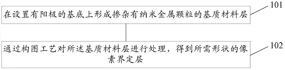
[0064] Corresponding to the organic electroluminescent device provided by the embodiment of the present invention, the embodiment of the present invention also provides a method for preparing an organic electroluminescent device, the method includes a method for preparing a pixel defining layer, such as image 3 As shown, the preparation method of the pixel defining layer includes:
[0065] 101. Form a matrix material layer doped with nano metal particles on a substrate provided with an anode.
[0066] Among them, the matrix material can be SiO 2 Particles, Polyimide, SiO 2 gel etc. The introduction of the nano-metal particles can be referred to the foregoing embodiments, and will not be repeated here.
[0067] 102. Process the matrix material layer through a patterning process to obtain a pixel defining layer of a desired shape.
[0068] In this step, the patterning process mainly refers to processing the matrix material through steps such as exposure, development and / or ...
Embodiment 1
[0100] Embodiment 1 contains Ag—SiO 2 Organic Electroluminescent Devices with Pixel Defining Layer
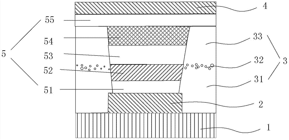
[0101] Such as figure 1 shown. Deposit a layer of SiO on a substrate 1 containing an anode 2 (such as ITO) by electron beam evaporation or vapor deposition 2 film31.
[0102] Then on SiO 2 The surface of the thin film 31 is coated with a 2nm thick silver layer by sputtering. During sputtering, the air pressure in the cavity is 10Pa, the atmosphere is argon, and the airflow is kept at 30sccm (standard-state cubic centimeter per mimute, standard-state cubic centimeter per minute), the sputtering current is 0.2A, the voltage is 0.5KV, and the substrate temperature is 200°C. Then place it under vacuum less than 1x10 -3 In a vacuum environment of Pa, anneal at a temperature of 300° C. for half an hour, and then cool to room temperature to form a discontinuous nano-silver particle layer 32 .
[0103] Then deposit a layer of SiO on the discontinuous nano-silver particle layer 3...
Embodiment 2
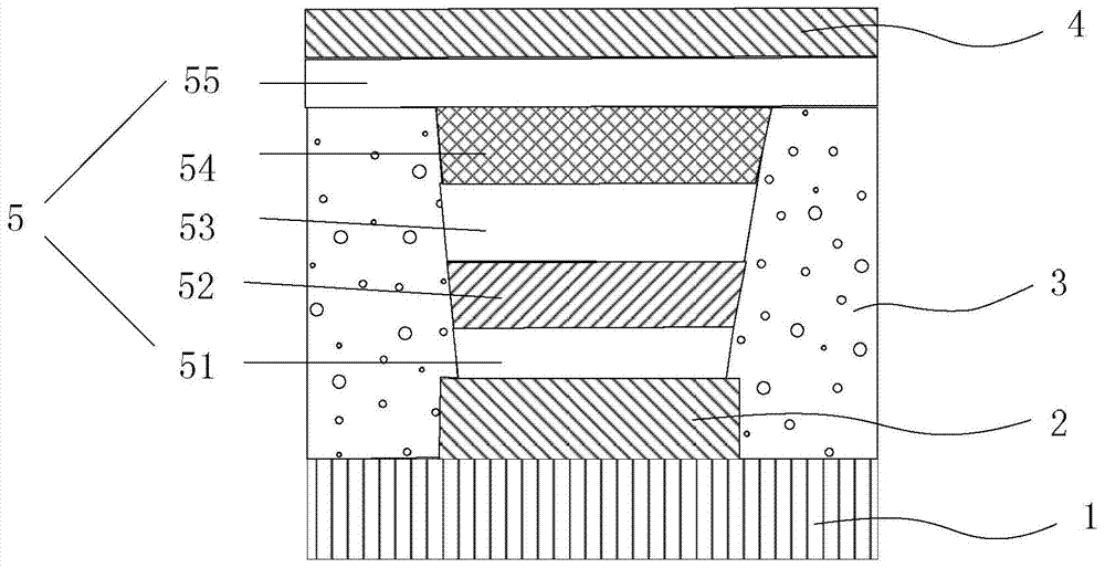
[0107] Embodiment 2 contains Au—SiO 2 Organic Electroluminescent Devices with Pixel Defining Layer
[0108] Such as figure 2 As shown, this embodiment adopts multi-target magnetron sputtering technology to prepare Au—SiO2 metal nanoparticles dispersed oxide 2 Composite film. In the double-target magnetron sputtering chamber, one target is placed with high-purity SiO 2 , one placed high-purity Au. The sputtering gas is high-purity argon (99.995%). The vacuum degree of the chamber before sputtering is -5 Pa, the sputtering pressure is 1.6×10 -1 Pa. The flow rates of argon and oxygen during sputtering were 8.3×10 -8 m 3 / s and 5.8×10 -8 m 3 / s, SiO 2 The RF power of Au and Au is 200W and 50W, respectively. By adjusting the opening of the shielding plate in front of the sputtering target, the ratio of materials deposited on the substrate can be selected, and finally Au-SiO with different doping ratios can be obtained. 2 Composite film.
[0109] Au-SiO by patterning ...
PUM
| Property | Measurement | Unit |
|---|---|---|
| Particle size | aaaaa | aaaaa |
| Thickness | aaaaa | aaaaa |
Abstract
Description
Claims
Application Information