Organic electroluminescence device packaging structure and method and display device

A technology of electroluminescent devices and packaging structures, which is applied in the direction of organic semiconductor devices, electric solid devices, electrical components, etc., can solve the problems of large internal stress, low elasticity of inorganic films, and peeling off, so as to improve the ability of blocking water and oxygen, Effect of extending life and improving reliability

Active Publication Date: 2014-01-01
BOE TECH GRP CO LTD
View PDF5 Cites 27 Cited by
  • Summary
  • Abstract
  • Description
  • Claims
  • Application Information

AI Technical Summary

Problems solved by technology

[0005] The existing thin film packaging technology is based on the multilayer film structure of organic polymer thin film and inorganic thin film alternately prepared by vacuum coating process. Among them, the inorganic thin film has high density and is the main water and oxygen barrier layer, but the inorganic thin film The elasticity is low, the internal stress is large, and it is relatively easy to be cracked by external force or peeled off from the OLED device. Therefore, an organic

Method used


Image

  • Organic electroluminescence device packaging structure and method and display device
  • Organic electroluminescence device packaging structure and method and display device

Examples


Embodiment 1

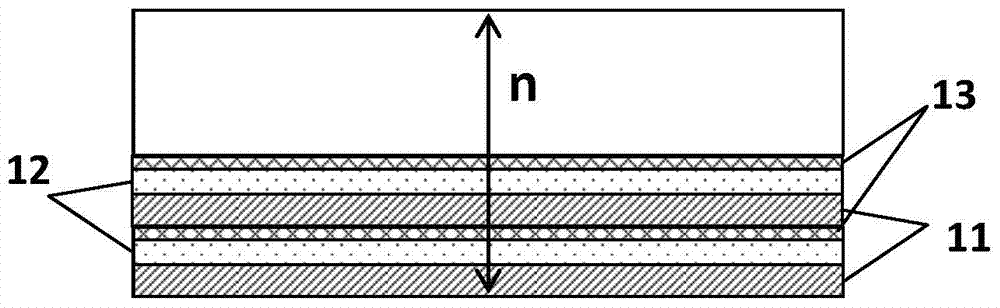
[0064] Example 1Al 2 o 3 (50nm) / PCP(50nm) / CFx(10nm)

[0065] The encapsulation method of the OLED device of the present embodiment comprises the following steps:

[0066] Step a: providing a substrate, which may be a quartz substrate or a glass substrate;

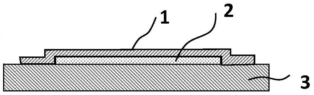
[0067] Step b: preparing the OLED device on the substrate;

[0068] Step c: Deposit a layer of Al on the substrate after step b by ion beam sputtering deposition 2 o 3 Thin films, the vacuum degree in the deposition chamber is 10 -6 Pa, deposition time is 10min, Al 2 o 3 The thickness of the film is 50nm;

[0069] Step d: using the method of chemical vapor deposition on the Al 2 o 3 Deposit a layer of polychlorinated p-xylene on the film, specifically, firstly sublimate the solid C-type polychlorinated-p-xylene at 100°C, and make the C-type polychlorinated-p-xylylene at 630°C on both sides The carbon-carbon bond of the chain is broken to generate a stable active monomer, and then the active monomer is introduced ...

Embodiment 2

[0072] Embodiment 2SiO (100nm) / polychlorinated p-xylene (200nm) / CFx (20nm)

[0073] The encapsulation method of the OLED device of the present embodiment comprises the following steps:

[0074] Step a: providing a substrate, which may be a quartz substrate or a glass substrate;

[0075] Step b: preparing the OLED device on the substrate;

[0076] Step c: Deposit a layer of SiO thin film on the substrate after step b by magnetron sputtering, and the vacuum degree in the deposition chamber is 10 -5 Pa, the deposition time is 10min, and the thickness of the SiO film is 100nm;

[0077] Step d: Deposit a layer of polychlorinated p-xylene on the SiO film by chemical vapor deposition, specifically, first sublimate the solid C-type polychlorinated-p-xylene at 100°C to make the C-type polychlorinated p-xylene The two side chain carbon-carbon bonds of substituted p-xylene are broken at 630°C to generate a stable active monomer, which is then introduced into the deposition chamber thr...

Embodiment 3

[0079] Embodiment 3SiON (100nm) / polychlorinated p-xylene (200nm) / CFx (20nm)

[0080] The encapsulation method of the OLED device of the present embodiment comprises the following steps:

[0081] Step a: providing a substrate, which may be a quartz substrate or a glass substrate;

[0082] Step b: preparing the OLED device on the substrate;

[0083] Step c: Deposit a layer of SiON film on the substrate after step b by magnetron sputtering, and the vacuum degree in the deposition chamber is 10 -5 Pa, the deposition time is 10min, and the thickness of the SiON film is 100nm;

[0084] Step d: Deposit a layer of polychlorinated p-xylene on the SiON film by chemical vapor deposition, specifically, first sublimate the solid C-type polychlorinated-p-xylene at 100°C to make the C-type polychlorinated p-xylene The two side chain carbon-carbon bonds of substituted p-xylene are broken at 630°C to generate a stable active monomer, which is then introduced into the deposition chamber thro...


PUM

PropertyMeasurementUnit
Thicknessaaaaaaaaaa
Thicknessaaaaaaaaaa

Abstract

The invention provides an organic electroluminescence device packaging structure and packaging method and a display device, and belongs to the field of organic electroluminescence. The organic electroluminescence device packaging structure comprises a substrate used for bearing an organic electroluminescence device, the organic electroluminescence device located on the substrate and at least one film packaging layer covering the organic electroluminescence device, wherein the film packaging layer is composed of an inorganic film, a fluorocarbon polymer film and an organic polymer film located between the inorganic film and the fluorocarbon polymer film. Through the organic electroluminescence device packaging structure and packaging method, the water oxygen blocking capacity of the film packaging layer can be effectively improved, and therefore the service life of the OLED device is effectively prolonged.

Description

technical field [0001] The invention relates to the field of organic electroluminescence, in particular to a packaging structure and packaging method of an organic electroluminescence device, and a display device. Background technique [0002] Organic electroluminescent device, also known as organic electroluminescent diode (OLED) device, is a new display technology, its display quality can be compared with thin film transistor liquid crystal display (TFT-LCD), and the price is far lower than it. Due to its remarkable advantages in flat panel display, such as high luminous brightness, rich colors, low-voltage DC drive, and simple manufacturing process, OLED has increasingly become a hot spot in international research. In less than 20 years, OLED has entered the stage of industrialization from research. [0003] OLED devices generally use a rigid glass substrate or a flexible polymer substrate as a carrier, and are composed of a transparent anode, a metal cathode, and two or...

Claims


Application Information

Patent Timeline
IPC IPC(8): H01L51/52H01L51/54H01L51/56
CPCH10K50/8445H10K50/844H10K71/00H10K85/111H10K2102/351
Inventor 尤娟娟
Owner BOE TECH GRP CO LTD
Why Eureka
Try Eureka