Semi-gate controlled source schottky barrier type tunneling field effect transistor

A technology of tunneling field effect and Schottky potential, which is applied in the direction of semiconductor devices, electrical components, circuits, etc., can solve the difficult and practical Schottky barrier MOSFETs transistors, the difficulty of forming Schottky barriers, and the weakened gate Electrode-to-source and drain electric field distribution and carrier distribution control capabilities, etc., to achieve the effects of low cost, reduced leakage current, and reduced process difficulty

Inactive Publication Date: 2014-01-08
SHENYANG POLYTECHNIC UNIV
View PDF4 Cites 23 Cited by
  • Summary
  • Abstract
  • Description
  • Claims
  • Application Information

AI Technical Summary

Problems solved by technology

And it is extremely difficult to form a Schottky barrier on the surface of a heavily doped extrinsic semiconductor, and the heavy doping itself also seriously weakens the gate's ability to cont

Method used


Image

  • Semi-gate controlled source schottky barrier type tunneling field effect transistor
  • Semi-gate controlled source schottky barrier type tunneling field effect transistor
  • Semi-gate controlled source schottky barrier type tunneling field effect transistor

Examples


Embodiment Construction

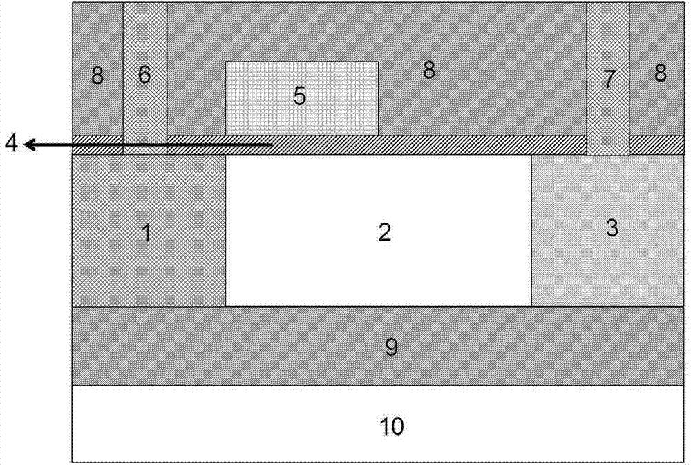
[0020] The invention provides a high-performance semi-gate controlled source Schottky barrier type tunneling field effect transistor, which does not need to introduce a narrow bandgap material as the tunneling part, but uses the source Schottky barrier The characteristic that the height is smaller than the forbidden band width of silicon can be realized by changing the voltage of the half-gate 5 to change the width of the source Schottky barrier formed by the metal source 1 and the intrinsic silicon 2 and the degree of energy band bending. Adjust the size of the transition ability of electrons or holes to the source Schottky barrier, and thus control the working current of the device. Therefore, the present invention realizes the improvement of the transition probability without introducing materials with a narrow bandgap width; at the same time, using the structural characteristics of the proposed half-gate 5 can significantly reduce the reverse leakage current while ensuring ...


PUM


Abstract

The invention relates to a semi-gate controlled source schottky barrier type tunneling field effect transistor. On the premise of no requirements on the introduction of a material such as a compound semiconductor, silicon germanide and germanium with a smaller forbidden bandwidth into the generation of a tunneling part of a device, a source schottky barrier is formed between a metal source and intrinsic silicon, and a semi-gate is used for controlling the barrier width of the source schottky barrier and the energy band bending degree of the intrinsic silicon to control the switching of the device. An asymmetrical semi-gate structural design is adopted, so that gate-induced drain leakage current is remarkably reduced on the premise of keeping gate voltage well controlling the width of the schottky barrier and the energy band bending degree. The semi-gate controlled source schottky barrier type tunneling field effect transistor has the advantages of process simplicity, low cost, high sub-threshold slope, high breakover current, low reverse leakage current and the like, and is suitable to be popularized and used.

Description

technical field [0001] The invention belongs to the field of ultra-large-scale integrated circuit manufacturing, and relates to a half-gate controlled source Schottky barrier type tunneling field-effect transistor suitable for ultra-high-integrated integrated circuit manufacturing. Background technique [0002] Currently, silicon-based PIN-type tunneling field-effect transistors (TFETs) may replace MOSFETs and become the next-generation VLSI logic unit due to their potential to have better switching characteristics and lower power consumption. or storage unit. However, compared with MOSFETs devices, its disadvantage is that the subthreshold slope only partially exceeds MOSFETs devices, and the forward conduction current is too small. And the structure of the region near the drain is similar to that of MOSFETs, so it still has a large gate-induced-drain leakage (GIDL) current when the gate is reverse-biased. In order to realize a tunneling field effect transistor with prac...

Claims


Application Information

Patent Timeline
IPC IPC(8): H01L29/739H01L29/47H01L29/423
CPCH01L29/7839H01L29/42356H01L29/47H01L29/66477
Inventor 靳晓诗刘溪揣荣岩
Owner SHENYANG POLYTECHNIC UNIV
Why Eureka
Try Eureka