Preparation method of silica-based CdZnTe film ultraviolet light detector

A detector and ultraviolet light technology, applied in the direction of semiconductor devices, final product manufacturing, sustainable manufacturing/processing, etc., to achieve the effect of simple growth process, low cost, and high feasibility of batch growth

Inactive Publication Date: 2014-01-08
SHANGHAI UNIV
View PDF3 Cites 11 Cited by
  • Summary
  • Abstract
  • Description
  • Claims
  • Application Information

AI Technical Summary

Problems solved by technology

At present, there has not been systematic research on the preparation process of detector-grade CdZnTe thin films and their detectors, especially heterojunction detectors at home and abroad.

Method used


Image

  • Preparation method of silica-based CdZnTe film ultraviolet light detector
  • Preparation method of silica-based CdZnTe film ultraviolet light detector
  • Preparation method of silica-based CdZnTe film ultraviolet light detector

Examples


Embodiment 1

[0024] The preparation process and steps of this embodiment are as follows:

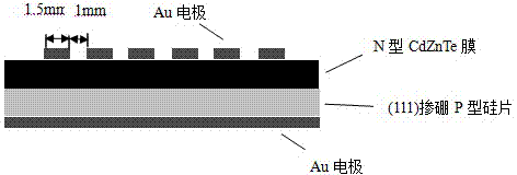
[0025] (a) Preparation of CdZnTe single crystal sublimation source: According to the known prior art, put high-purity Cd, Zn, Te into a quartz tube, and use moving heating method to grow under high vacuum. Uniform CdZnTe single crystal, wherein the molar content of zinc is 5%, the molar content of Cd is 43%, and the molar content of Te is 52%, and the grown crystal slice is used as the sublimation source;

[0026] (b) Substrate pretreatment: Boron-doped (111) P-type silicon was used as the substrate, and the substrate was ultrasonically cleaned with deionized water, acetone and ethanol for 15 minutes to remove impurities and organic substances on the surface, and dried Put it into the near space sublimation reaction chamber;

[0027] (c) CdZnTe thin film growth process: Turn on the mechanical pump to evacuate the sublimation chamber to below 3Pa, then turn off the mechanical pump, pass in argon ...

Embodiment 2

[0032] The preparation process and steps of this embodiment are as follows:

[0033] (a) Preparation of CdZnTe single crystal sublimation source: According to the known prior art, put high-purity Cd, Zn, Te into a quartz tube, and use moving heating method to grow under high vacuum. Uniform CdZnTe single crystal, wherein the molar content of zinc is 5%, the molar content of Cd is 43%, and the molar content of Te is 52%, and the grown crystal slice is used as the sublimation source;

[0034] (b) Substrate pretreatment: Boron-doped (111) P-type silicon was used as the substrate, and the substrate was ultrasonically cleaned with deionized water, acetone and ethanol for 15 minutes to remove impurities and organic substances on the surface, and dried Put into the close space sublimation reaction chamber.

[0035](c) CdZnTe film growth process: Turn on the mechanical pump to evacuate the sublimation chamber to below 3Pa, then turn off the mechanical pump, feed argon gas to adju...

Embodiment 3

[0039] The preparation process and steps of this embodiment are as follows:

[0040] (a) Preparation of CdZnTe single crystal sublimation source: According to the known prior art, put high-purity Cd, Zn, Te into a quartz tube, and use moving heating method to grow under high vacuum. Uniform CdZnTe single crystal, wherein the molar content of zinc is 5%, the molar content of Cd is 43%, and the molar content of Te is 52%, and the grown crystal slice is used as the sublimation source;

[0041] (b) Substrate pretreatment: Boron-doped (111) P-type silicon was used as the substrate, and the substrate was ultrasonically cleaned with deionized water, acetone and ethanol for 15 minutes to remove impurities and organic substances on the surface, and dried Put into the close space sublimation reaction chamber.

[0042] (c) CdZnTe film growth process: turn on the mechanical pump to evacuate, pump the air pressure in the sublimation chamber to below 3Pa, then turn off the mechanical p...


PUM


Abstract

The invention relates to a preparation method of a silica-based CdZnTe thin film ultraviolet light detector, which belongs to the technical field of ultraviolet light detector light-sensitive material and device manufacturing process. A near-space sublimation method is adopted, an N-type CdZnTe thin film is prepared on a P-type Si substrate, an ultraviolet light detector with a CdZnTe thin film/Si heterogeneous structure is formed, and a new method is provided for manufacturing the ultraviolet light detector with high performance. The invention relates to the silicon substrate-based heterojunction CdZnTe thin film ultraviolet light detector, which is characterized in that a CdZnTe thin film sample with high smoothness, uniform particle size and high quality is prepared on a Si chip by adopting the near-space sublimation method, and the prepared heterojunction detector has high sensitivity.

Description

technical field [0001] The invention relates to a method for preparing a heterojunction CdZnTe thin film ultraviolet light detector based on a silicon substrate, and belongs to the technical field of ultraviolet light detector photosensitive materials and device manufacturing techniques. Background technique [0002] Ultraviolet detection technology is the most popular photoelectric detection technology for both military and civilian purposes in recent years. Because space, flames, oil, gas pollutant molecules, and the corona phenomenon of high-voltage lines all contain ultraviolet radiation, ultraviolet detectors have a wide range of application requirements in aerospace, communication, civil detection and other fields. Countries all over the world have listed solid-state ultraviolet detector technology as a key topic of current research and development. In the research of wide-bandgap semiconductor ultraviolet detectors, the past decade has mainly focused on materials suc...

Claims


Application Information

Patent Timeline
Patent Type & Authority Applications(China)
IPC IPC(8): H01L31/18
CPCH01L31/1832H01L31/1836Y02P70/50
Inventor 王林军姚蓓玲周捷沈萍史冬良黄健唐可张凯勋
Owner SHANGHAI UNIV
Why Eureka
Try Eureka