

Method for preparing TiN through utilizing physical vapor deposition (PVD)
A technology of titanium nitride and wafers, applied in the field of PVD preparation of TiN thin films
- Summary
- Abstract
- Description
- Claims
- Application Information
AI Technical Summary
Problems solved by technology
Method used
Image

Examples
Embodiment Construction
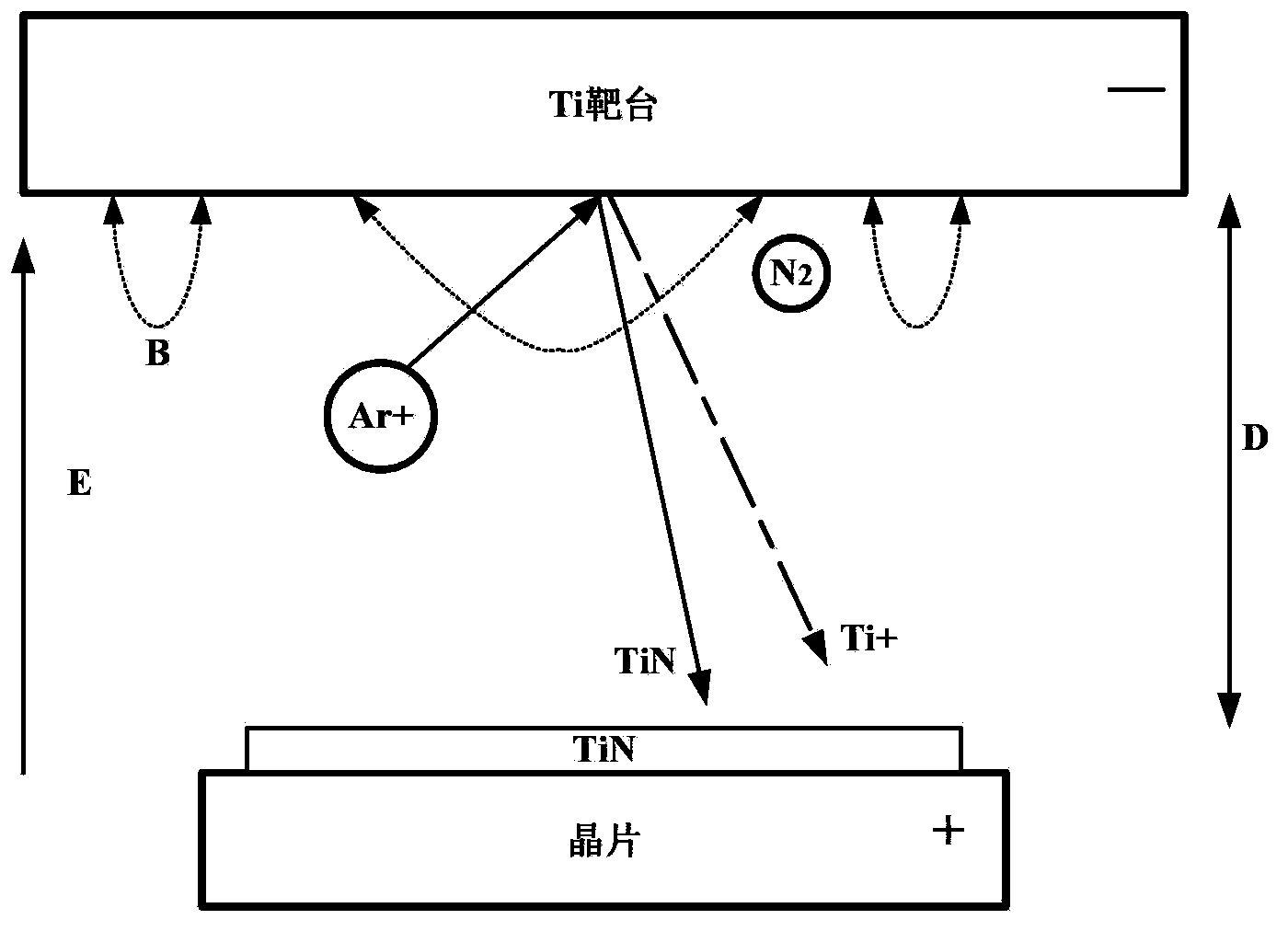
[0017] The features and technical effects of the technical solution of the present invention will be described in detail below with reference to the accompanying drawings and in combination with schematic embodiments, and a method for preparing TiNx by PVD is disclosed. It should be pointed out that similar reference numerals represent similar structures, and the terms "first", "second", "upper", "lower" and the like used in this application can be used to modify various device structures or manufacturing processes . These modifications do not imply spatial, sequential or hierarchical relationships of the modified device structures or fabrication processes unless specifically stated.
[0018] In the present invention, general-purpose (magnetron) sputtering equipment can be used to complete the preparation of TiNx. It is worth noting that in the following text of this application, for the sake of simplicity, sometimes the nitride of titanium (titanium nitride) is referred to s...
PUM
| Property | Measurement | Unit |
|---|---|---|
| thickness | aaaaa | aaaaa |
Abstract
Description
Claims
Application Information