Alkaline texturing process for monocrystalline silicon wafers

A single crystal silicon wafer and process technology, applied in the field of solar cells, can solve the problems of difficult conductive paste and inability to spread uniformly, achieve the effect of easier control of thickness, ensure uniform spread, and be beneficial to sintering

Active Publication Date: 2015-10-21
HENGDIAN GRP DMEGC MAGNETICS CO LTD
View PDF3 Cites 0 Cited by
  • Summary
  • Abstract
  • Description
  • Claims
  • Application Information

AI Technical Summary

Problems solved by technology

[0004] The purpose of the present invention is to solve the problem that the structure size and arrangement of the suede surface obtained by the alkaline texturizing process in the prior art are random, and the secondary reflection cannot be well formed in an all-round way, and the diffusion cannot be uniformly diffused, and it is difficult to form a good contact with the conductive paste. In order to solve the problem of contact, a single-crystal silicon chip alkaline texture-making process with simple process steps, suitable for industrial production and low cost is provided. The texture structure obtained by the present invention is an inverted pyramid structure with regular size and arrangement, which can be easily Good overall formation of secondary reflection, while ensuring uniform diffusion, is conducive to the coating of conductive paste, making the thickness of conductive paste easier to control, good contact with conductive paste, conducive to sintering of metals, and reducing contact resistance

Method used


Image

  • Alkaline texturing process for monocrystalline silicon wafers
  • Alkaline texturing process for monocrystalline silicon wafers
  • Alkaline texturing process for monocrystalline silicon wafers

Examples


Embodiment 1

[0032] (a) Removing the damaged layer: the single crystal silicon wafer 1 was placed in a NaOH solution with a mass concentration of 12%, etched at 100°C for 45s, then washed with deionized water and dried.

[0033] (b) Mask preparation: put the single crystal silicon wafer 1 with the damaged layer removed into an oxidation furnace to oxidize, and form SiO with a thickness of 10 nm on the surface of the single crystal silicon wafer 1 2 Mask 2.

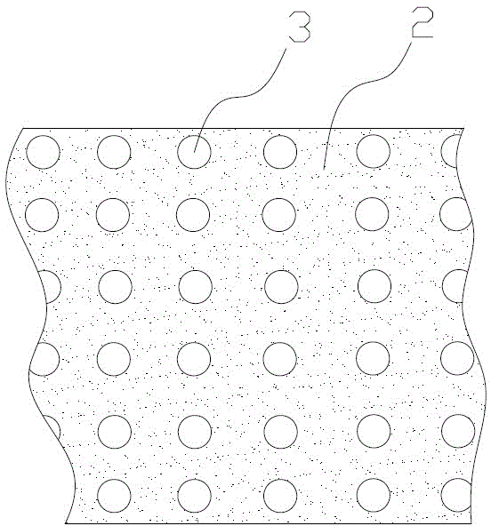
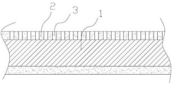
[0034] (c) Mask opening: for the formation of SiO 2 Laser window opening is carried out on the surface of the single crystal silicon wafer 1 of the mask 2, so that the SiO 2 Fenestration holes 3 evenly spaced are formed on the mask 2 (see figure 1 , figure 2 ), the fenestration interval is 8 μm, and the pore diameter is 4 μm.

[0035] (d) Texturing the surface: Put the window-opened monocrystalline silicon wafer 1 in a NaOH solution with a mass concentration of 25%, and corrode it at 100°C for 60 minutes, so that the surface of th...

Embodiment 2

[0038] (a) Removing the damaged layer: the single crystal silicon wafer 1 was placed in a NaOH solution with a mass concentration of 16%, etched at 70°C for 30s, then washed with deionized water and dried.

[0039] (b) Mask preparation: put the single crystal silicon wafer 1 with the damaged layer removed into an oxidation furnace to oxidize, and form SiO with a thickness of 100 nm on the surface of the single crystal silicon wafer 1 2 Mask 2.

[0040] (c) Mask opening: for the formation of SiO 2 Laser window opening is carried out on the surface of the single crystal silicon wafer 1 of the mask 2, so that the SiO 2 Fenestration holes 3 evenly spaced are formed on the mask 2 (see figure 1 , figure 2 ), the window opening interval is 5m, and the aperture is 3m.

[0041] (d) Texturing the surface: place the windowed monocrystalline silicon wafer 1 in a NaOH solution with a mass concentration of 20, and etch at 80°C for 40 minutes to form an inverted pyramid-structured textu...

Embodiment 3

[0044] (a) Removing the damaged layer: the single crystal silicon wafer 1 was placed in a NaOH solution with a mass concentration of 13%, etched at 800°C for 50s, then washed with deionized water and dried.

[0045] (b) Mask preparation: put the single crystal silicon wafer 1 with the damaged layer removed into an oxidation furnace to oxidize, and form SiO with a thickness of 200 nm on the surface of the single crystal silicon wafer 1 2 Mask 2.

[0046] (c) Mask opening: for the formation of SiO 2 Laser window opening is carried out on the surface of the single crystal silicon wafer 1 of the mask 2, so that the SiO 2 Fenestration holes 3 evenly spaced are formed on the mask 2 (see figure 1 , figure 2 ), the fenestration interval is 4 μm, and the pore diameter is 2 μm.

[0047] (d) Texturing the surface: Place the window-opened monocrystalline silicon wafer 1 in an NaOH solution with a mass concentration of 18%, and corrode it at 70°C for 20 minutes, so that the surface of...


PUM

PropertyMeasurementUnit
thicknessaaaaaaaaaa
thicknessaaaaaaaaaa
thicknessaaaaaaaaaa

Abstract

The invention discloses an alkaline type texturing process of monocrystalline silicon wafer, which is used for solving the problems that secondary reflection cannot be completely formed very well and good contact with conductive slurry is difficult to form due to uneven diffusion as size and arrangement of a textured surface obtained by the alkaline type texturing process in the prior art are random. The alkaline type texturing process mainly comprises the following steps: (a) removing an affected layer; (b) preparing a mask; (c) windowing the mask; (d) texturing on a surface; and (e) removing the mask. The alkaline type texturing process disclosed by the invention is simple in step, suitable for industrial production and low in cost; the obtained monocrystalline silicon wafer textured structure is an inverted pyramid structure with regular size and arrangement, so that secondary reflection can be completely formed very well; and meanwhile, diffusion is guaranteed to be uniform and coating of conductive slurry is facilitated, so that thickness of the conductive slurry is controlled easier, contact with the conductive slurry is good, metal sintering is facilitated, and contact resistance is reduced.

Description

technical field [0001] The invention relates to the technical field of solar cells, in particular to an alkaline texturing process for single crystal silicon wafers. Background technique [0002] In the production of conventional solar monocrystalline silicon cells, the traditional alkaline texturing process is generally adopted, that is, through the reaction of the silicon wafer and the alkaline texturizing solution to form "pyramid"-shaped undulations on the surface of the silicon wafer, through the texture of these pyramid structures Surface to form secondary reflection, improve light absorption, reduce the reflectivity of the silicon wafer surface, thereby improving the conversion efficiency of the cell. [0003] For example, the Chinese patent with application publication number CN102703903A and application publication date of 2012.10.03 discloses an alkali texturing process, the main steps of which are as follows: first, silicon wafers are etched in an alkaline soluti...

Claims


Application Information

Patent Timeline
Patent Type & Authority Patents(China)
IPC IPC(8): C30B33/10H01L31/18C23F1/32C23F1/02
CPCY02P70/50
Inventor 韩健鹏吴敏
Owner HENGDIAN GRP DMEGC MAGNETICS CO LTD
Why Eureka
Try Eureka