A kind of semiconductor structure and its forming method

A semiconductor and shallow trench isolation technology, which is applied in semiconductor devices, semiconductor/solid-state device manufacturing, electrical components, etc., can solve problems affecting device performance and achieve the effects of improving performance and reducing free oxygen concentration

Active Publication Date: 2016-03-23
SEMICON MFG INT (SHANGHAI) CORP
View PDF4 Cites 0 Cited by
  • Summary
  • Abstract
  • Description
  • Claims
  • Application Information

AI Technical Summary

Problems solved by technology

[0005] The purpose of the present invention is to provide a semiconductor structure and its formation method to solve the situation in the prior art that the high-K dielectric layer is adversely affected and affects the performance of the device

Method used


Image

  • A kind of semiconductor structure and its forming method
  • A kind of semiconductor structure and its forming method
  • A kind of semiconductor structure and its forming method

Examples


Embodiment Construction

[0030] The method for forming the semiconductor structure provided by the present invention will be further described in detail below with reference to the accompanying drawings and specific embodiments. Advantages and features of the present invention will be apparent from the following description and claims. It should be noted that all the drawings are in a very simplified form, and are only used for the purpose of conveniently and clearly assisting in describing the embodiments of the present invention.

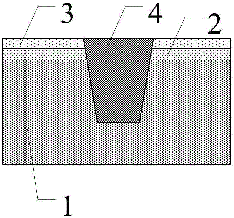
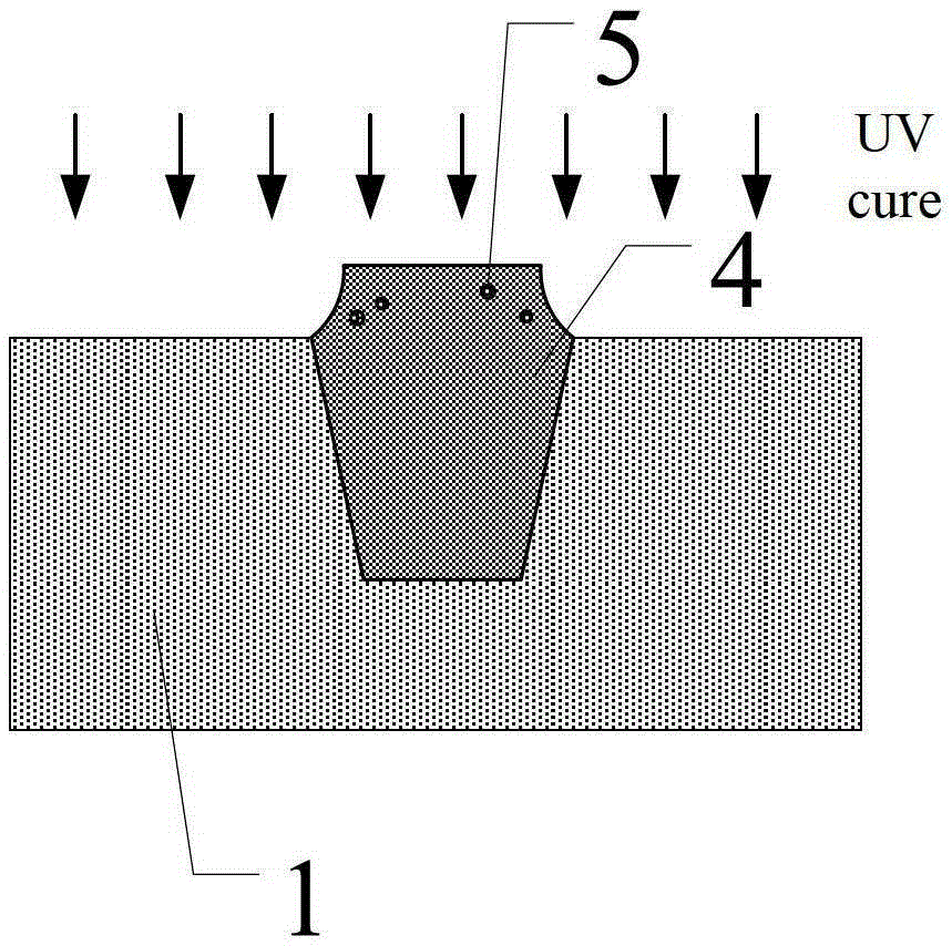
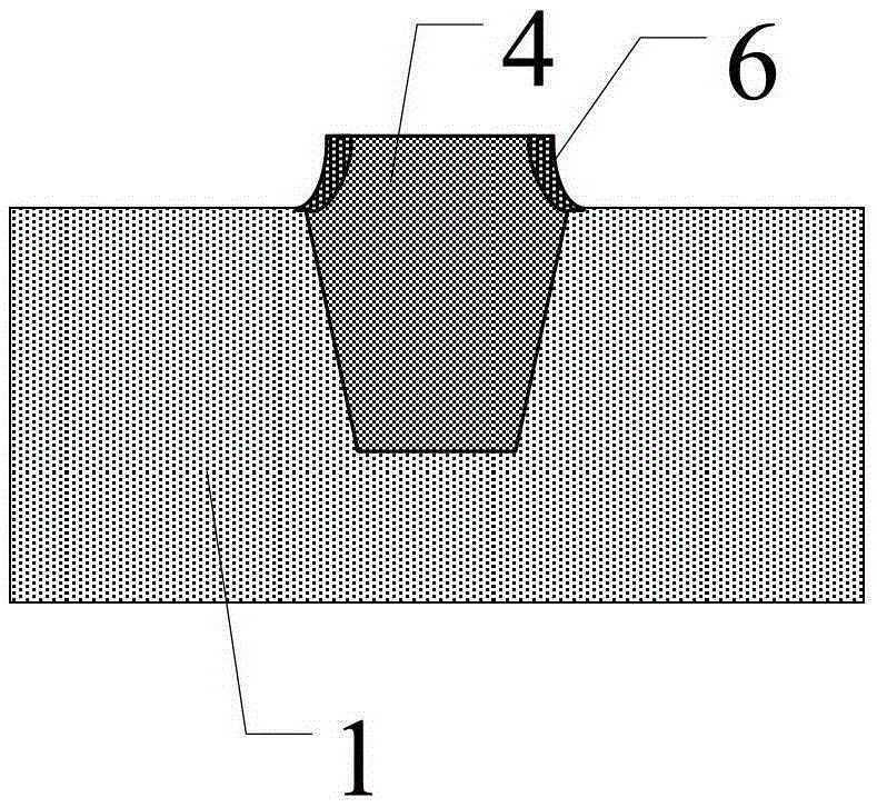
[0031] A process for forming a semiconductor structure, including: Please refer to figure 1 , providing a substrate 1 ; forming shallow trench isolation 4 in the substrate 1 . Specifically, the following process steps are adopted: an active area oxide layer 2 and an active area mask layer 3 are deposited on the substrate 1, the active area oxide layer 2 is usually silicon dioxide, and the active area mask layer 3 It can be silicon nitride, etc., and then use a photolit...


PUM


Abstract

The invention discloses a semi-conductor structure and a forming method thereof. Shallow channel isolation is processed in an ultraviolet irradiating method, so that the concentration of free oxygen in the shallow channel isolation is greatly reduced, a blocking layer is formed, diffusion of the free oxygen is further prevented, a high K dielectric layer cannot be eroded by the free oxygen, large leak currents are avoided, shift of a threshold voltage Vt can be effectively controlled, and performance of a component is improved.

Description

technical field [0001] The invention relates to the field of integrated circuit manufacturing, in particular to a semiconductor structure capable of avoiding damage to a high-K dielectric layer and a forming method thereof. Background technique [0002] As the size of transistors continues to shrink, HKMG (high-K dielectric layer + metal gate) technology has almost become an essential technology for processes below 45nm. Due to its large dielectric constant, the high-K dielectric layer can achieve the same equivalent oxide thickness (EOT: equivalent oxide thickness) as silicon dioxide, and its actual thickness is much larger than silicon dioxide, so it is deeply loved Industry welcome. [0003] However, most high-K materials are ionic metal oxides. This basic material characteristic may cause many unreliable problems when high-K materials are used as dielectric layers. [0004] In the actual production process, due to the etching process, etc., there will be more free oxyg...

Claims


Application Information

Patent Timeline
Patent Type & Authority Patents(China)
IPC IPC(8): H01L21/762H01L29/06
CPCH01L21/02348H01L21/02362H01L21/76224
Inventor 张彬
Owner SEMICON MFG INT (SHANGHAI) CORP
Why Eureka
Try Eureka