GaAs nanowire array photocathode and manufacturing method thereof

A nanowire array and photocathode technology, which is applied in the manufacture of light-emitting cathodes, photoemission cathodes, nanotechnology, etc., to achieve the effects of improved detection efficiency, sufficient photon absorption, and good repeatability

Inactive Publication Date: 2014-02-19
EAST CHINA UNIV OF TECH
View PDF3 Cites 16 Cited by
  • Summary
  • Abstract
  • Description
  • Claims
  • Application Information

AI Technical Summary

Problems solved by technology

[0004] Aiming at the deficiencies of existing traditional thin film materials in photon absorption and elec

Method used


Image

  • GaAs nanowire array photocathode and manufacturing method thereof
  • GaAs nanowire array photocathode and manufacturing method thereof
  • GaAs nanowire array photocathode and manufacturing method thereof

Examples


Embodiment Construction

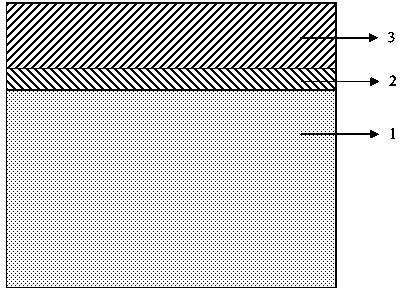
[0027] figure 1 Schematic diagram of the structure of the GaAs nanowire array photocathode. As shown in the figure, the required nanowire array is prepared on the GaAs substrate by photolithography plus dry etching technology. In the figure, the GaAs nanowire array is arranged periodically and neatly. When light is incident, the light will be continuously absorbed, reflected and refracted in the GaAs nanowire array until most of it is absorbed. In order to prepare high-quality GaAs nanowires, a layer of SiO was grown on the GaAs substrate by PECVD technology. 2 The barrier layer is used to protect the mask from being damaged during ICP etching. RTP technology is used to process GaAs nanowires to eliminate nanowire defects or lattice damage caused by the etching process and improve the integrity of the GaAs nanowire lattice structure. GaAs nanowires have a diameter of 4 μm, a height of 9 μm, and a p-type doping concentration of 1×10 19 cm -3 , the shape of the nanowire is...


PUM

PropertyMeasurementUnit
Thicknessaaaaaaaaaa
Diameteraaaaaaaaaa
Dislocation densityaaaaaaaaaa

Abstract

The invention discloses a GaSa nanowire array photocathode and a manufacturing method of the GaSa nanowire array photocathode. The cathode is composed of a GaSa substrate layer, A GaSa nanowire array emission layer and a Cs/O activation layer. The method includes the steps that GaSa nanowire array material is manufactured on a GaSa substrate with a certain thickness by the adoption of a dry etching technology, the GaSa nanowire array photocathode is manufactured in an ultrahigh vacuum activation system, after the GaSa nanowire material is activated to be the photocathode, and a Cs-O layer is adsorbed around whole nanowires to generate negative electron affinity, so that an energy band structure is formed on the GaSa nanowires with the middle higher than the periphery. A nanowire array structure is beneficial to photon absorption, and the nanowire photocathode energy band structure is beneficial to photoelectronic emission, so that photon absorption and electron emission efficiency of the material is improved.

Description

technical field [0001] The invention relates to the technical field of photoelectric emission materials, in particular to a nanowire array photocathode obtained from a GaAs compound semiconductor material through a dry etching technique and a preparation method thereof. Background technique [0002] A photocathode is a photoemissive material that converts light signals into electrical signals by using the external photoelectric effect. GaAs photocathode with negative electron affinity has been widely used in the fields of photodetection and imaging due to its many advantages such as high quantum efficiency, small dark emission, high energy and spatial resolution, high emission current density, and uniform planar electron emission. widely used. [0003] Generally, the photocathode is made of thin film materials. The thin film materials have the advantages of mature material growth process and good film quality, but the reflectivity of the thin film materials is relatively hi...

Claims


Application Information

Patent Timeline
IPC IPC(8): H01J1/34H01J9/12B82Y40/00
Inventor 邹继军郭栋朱志甫彭新村邓文娟王炜路冯林张益军常本康
Owner EAST CHINA UNIV OF TECH
Why Eureka
Try Eureka