Multi-gate SOI-LDMOS device structure

A device structure and gate structure technology, applied in semiconductor devices, electrical components, circuits, etc., can solve the problems of transconductance characteristics, forward conduction resistance, self-heating effect, poor radiation resistance, etc., and achieve improved radiation resistance, The effects of small forward conduction resistance and high radiation resistance

Inactive Publication Date: 2014-02-19
SHANGHAI INST OF MICROSYSTEM & INFORMATION TECH CHINESE ACAD OF SCI +1
View PDF3 Cites 15 Cited by
  • Summary
  • Abstract
  • Description
  • Claims
  • Application Information

AI Technical Summary

Problems solved by technology

[0007] In view of the above-mentioned shortcoming of the prior art, the object of the present invention is to provide a multi-gate SOI-LDMOS device structure, w...

Method used


Image

  • Multi-gate SOI-LDMOS device structure
  • Multi-gate SOI-LDMOS device structure
  • Multi-gate SOI-LDMOS device structure

Examples


Embodiment 1

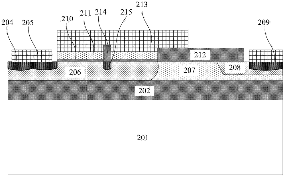
[0048] Such as figure 2 As shown, this embodiment provides a multi-gate SOI-LDMOS device structure, including at least:

[0049] SOI substrate, including silicon substrate 201, buried oxide layer 202 and top silicon layer;

[0050] Active regions 204 and 205 are formed in the top silicon layer, including source regions 204 and 205, channel regions 206, drift regions 207, lightly doped drain regions 208, and drain regions 209 connected in sequence;

[0051] A polysilicon gate, including a gate oxide layer 210 and a polysilicon layer 211 bonded to the surface of the channel region 206, the polysilicon gate is separated into at least two short gate structures by at least one dielectric layer 214, and corresponds to the bottom of the dielectric layer 214 A heavily doped region 215 of an opposite doping type to that of the channel region 206 is formed in the channel region 206 .

[0052] The source regions 204 and 205, as an example, include that the source regions 204 and 205 i...

Embodiment 2

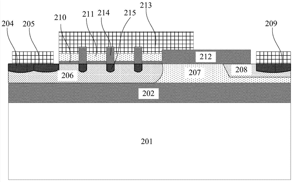
[0061] Such as image 3 As shown, this embodiment provides a multi-gate SOI-LDMOS device structure, including at least:

[0062] SOI substrate, including silicon substrate 201, buried oxide layer 202 and top silicon layer;

[0063] Active regions 204 and 205 are formed in the top silicon layer, including source regions 204 and 205, channel regions 206, drift regions 207, lightly doped drain regions 208, and drain regions 209 connected in sequence;

[0064] A polysilicon gate, including a gate oxide layer 210 and a polysilicon layer 211 bonded to the surface of the channel region 206, the polysilicon gate is separated into at least two short gate structures by at least one dielectric layer 214, and corresponds to the bottom of the dielectric layer 214 A heavily doped region 215 of an opposite doping type to that of the channel region 206 is formed in the channel region 206 .

[0065] The source regions 204 and 205, as an example, include that the source regions 204 and 205 in...

Embodiment 3

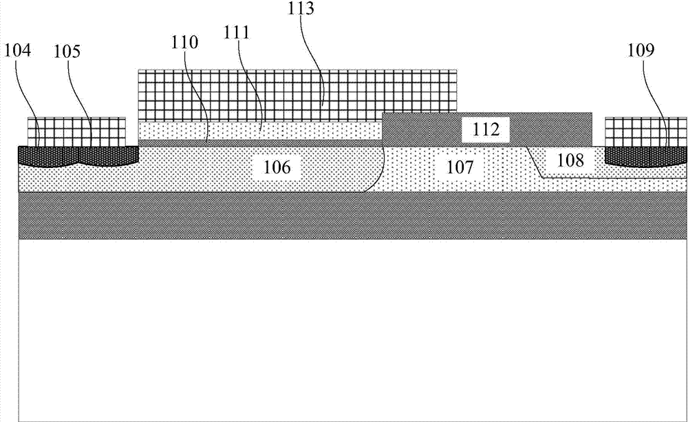
[0080] This embodiment provides a multi-gate SOI-LDMOS device structure, the basic structure of which is as in Embodiment 1, wherein the source region includes a heavily doped N-type region and a heavily doped P-type region, and the heavily doped P type region is connected to the channel region; the doping type of the channel region is N type, the doping type of the drift region, shallow doped drain and drain region is P type, and the heavily doped region The doping type is P-type.


PUM

PropertyMeasurementUnit
Lengthaaaaaaaaaa

Abstract

The invention provides a multi-gate SOI-LDMOS device structure which comprises an SOI substrate, an active region and a polysilicon gate. The SOI substrate comprises a silicon substrate body, an oxygen buried layer and a top silicon layer, the active region is formed in the top silicon layer and comprises a source region, a channel region, a drift region, a shallow doping drain region and a drain region, the source region, the channel region, the drift region, the shallow doping drain region and the drain region are sequentially connected, the polysilicon gate comprises a gate-oxide layer and a polysilicon layer, the gate-oxide layer is combined to the surface of the channel region, the polysilicon gate is separated by at least one dielectric layer into two short gate structures, and heavy doping regions inversed with the channel region in doping type are formed corresponding to the position, below the dielectric layer, in the channel region. The multi-gate SOI-LDMOS device structure has the advantages of being high in breakdown voltage, good in transconductance characteristic, small in positive break-over resistance, low in self-heating effect and the like. As the heavy doping regions inversed with the channel region in doping type are formed between short gates, when a device is irradiated, the heavy doping regions serve as recombination centers, the large number of recombination centers are provided for electron hole pairs generated by irradiation, and the whole radiation resisting performance of the device is accordingly improved.

Description

technical field [0001] The invention relates to a semiconductor device structure, in particular to a multi-gate SOI-LDMOS device structure. Background technique [0002] Contemporary power integrated circuits are widely used in daily consumption fields such as power control systems, automotive electronics, display device drivers, communications and lighting, as well as in many important fields such as national defense and aerospace. With the continuous expansion of its application fields, the high voltage of its core parts The requirements for devices are getting higher and higher. In particular, it is required to reduce the on-resistance of the device as much as possible under the premise of ensuring the breakdown voltage to improve device performance and reduce power consumption. Traditional high-voltage devices have a "silicon limit" relationship (Ron,sp∞BV 2.5 ), as the breakdown voltage of the device increases, the specific on-resistance of the device increases sharply...

Claims


Application Information

Patent Timeline
IPC IPC(8): H01L29/78H01L29/06H01L29/423
Inventor 赵清太徐大伟西格弗里德曼特尔俞跃辉程新红
Owner SHANGHAI INST OF MICROSYSTEM & INFORMATION TECH CHINESE ACAD OF SCI
Why Eureka
Try Eureka