MEMS pressure sensor chip based on SOI technology and manufacturing method thereof

A pressure sensor and technology, applied in the field of micro-electromechanical systems (MEMS), can solve the problems of poor sensor repeatability and hysteresis, and achieve the effects of good repeatability and stability, high sensitivity, and improved operating temperature range

Active Publication Date: 2014-02-26
SHENYANG POLYTECHNIC UNIV
View PDF3 Cites 27 Cited by
  • Summary
  • Abstract
  • Description
  • Claims
  • Application Information

AI Technical Summary

Problems solved by technology

However, due to the use of polysilicon strain resistance, the performance of the sensor such as repeatability and hysteresis is poor

Method used


Image

  • MEMS pressure sensor chip based on SOI technology and manufacturing method thereof
  • MEMS pressure sensor chip based on SOI technology and manufacturing method thereof
  • MEMS pressure sensor chip based on SOI technology and manufacturing method thereof

Examples


Embodiment 1

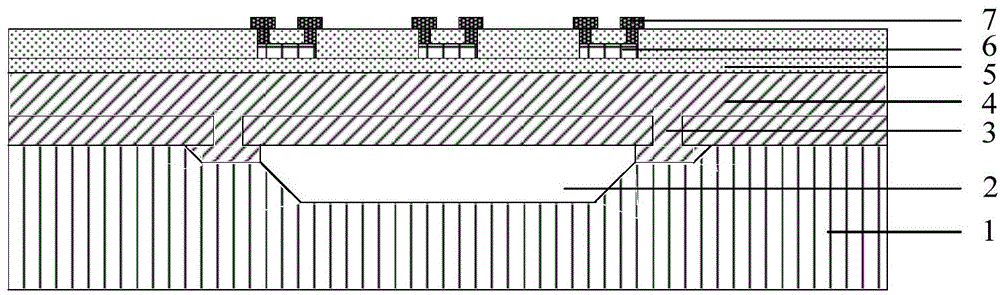
[0059] Manufacturing methods of MEMS pressure sensors based on SOI technology, such as Figure 2~Figure 9 As shown, the specific steps are:

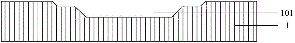
[0060] (1) Using isotropic etchant HNA (hydrofluoric acid / nitric acid / acetic acid) on the single crystal silicon substrate to form a stepped groove through two photolithography and etching, the result is as follows image 3 shown;

[0061] (2) Using PECVD to deposit silicon dioxide as the sacrificial layer 101 on the single crystal silicon substrate with stepped grooves, the substrate was restored to flatness by polishing, and the silicon dioxide in the area outside the groove was removed at the same time, the result Such as Figure 4 shown;

[0062] (3) Using LPCVD to deposit a layer of polysilicon to form the first layer of polysilicon 103, dry etching after annealing to form the cavity etching hole 3, the result is as follows Figure 5 shown;

[0063] (4) The chip is placed in a hydrofluoric acid solution to remove the silicon di...


PUM


Abstract

The invention discloses an MEMS pressure sensor chip based on an SOI technology and a manufacturing method of the MEMS pressure sensor chip. The MEMS pressure sensor chip is suitable for absolute pressure measurement and comprises a monocrystalline silicon substrate. A flat elastic membrane is arranged on a groove of the monocrystalline silicon substrate. The edge of the elastic membrane is provided with corrosion holes. The elastic membrane and the groove of the silicon substrate form an airtight cavity. Four monocrystalline silicon strain resistors are arranged on the elastic membrane. All the monocrystalline silicon strain resistors are isolated from one another through insulating media, and the monocrystalline silicon strain resistors are also isolated from the elastic membrane through insulating media. The four strain resistors are connected through metal wires to form a Wheatstone bridge so as to convert pressure into a voltage and output the voltage. The MEMS pressure sensor chip has the advantages of being small in size, good in repeatability and hysteresis, high in sensitivity, wide in operating temperature range, and the like; besides, the manufacturing technique is compatible with the integrated circuit technique.

Description

technical field [0001] The invention mainly relates to a MEMS pressure sensor based on SOI (silicon on insulating substrate) technology and a manufacturing method thereof, belonging to the field of micro-electromechanical systems (MEMS). Background technique [0002] At present, the widely used semiconductor pressure sensor is silicon cup structure diffused silicon pressure sensor. The force sensitive bridge of this sensor adopts p-type single crystal silicon strain resistance, and the elastic film is formed by etching silicon cup on n-type silicon substrate. The gap between the resistor and the elastic film is isolated by the reverse-biased pn junction. When the operating temperature exceeds 120°C, the leakage current of the pn junction will intensify, which will seriously invalidate the sensor characteristics, so it is not suitable for working under high temperature conditions. If dielectric isolation is used, the maximum operating temperature of the sensor can be increas...

Claims


Application Information

Patent Timeline
Patent Type & Authority Applications(China)
IPC IPC(8): G01L1/22B81B3/00B81C1/00
Inventor 揣荣岩王健郭浩赵豪
Owner SHENYANG POLYTECHNIC UNIV
Why Eureka
Try Eureka