Silicon chip thinning method

A silicon wafer, thinning rate technology, applied in the direction of electrical components, circuits, semiconductor/solid-state device manufacturing, etc., can solve the problems of reducing the lifetime of minority carriers, large leakage current, low injection efficiency, etc., to reduce crystal defects and surface damage and Effects of cracks, defect reduction, heat and stress reduction

Active Publication Date: 2014-02-26
中国东方电气集团有限公司
View PDF6 Cites 32 Cited by
  • Summary
  • Abstract
  • Description
  • Claims
  • Application Information

AI Technical Summary

Problems solved by technology

[0005] In order to overcome the problems that the existing silicon wafer thinning methods affect the quality of silicon wafers, cause large leakage current, low injection efficiency, and reduce the lifetime of minority carriers, it is now proposed that it can not only ensure the batch thinning of silicon wafers, but also effectively A silicon wafer thinning method that minimizes the backside defects caused by thinning

Method used


Image

  • Silicon chip thinning method

Examples


Embodiment 1

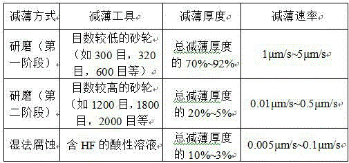
[0023] A method for thinning a silicon wafer. In step 1, a protective material is arranged on the front side of the silicon wafer; in step 2, the back side of the silicon wafer is thinned by grinding in stages. The specific thinning process is divided into two stages: In the first stage, the silicon wafer is thinned with a 300-600 mesh grinding wheel, and the thickness subtracted at this stage is d 1 , the thinning rate is v 1 In the second stage, the 1200-2000 mesh grinding wheel is used to thin the silicon wafer. In this stage, a low-speed grinding and thinning is adopted, and the thinning rate is v 2 , the thickness d of the first-stage thinning 1 is 70%~92% of the total thinning thickness d, the first stage thinning rate v 1 =1μm / s to 5μm / s, the second-stage thinned thickness d 2 It is 20%~5% of the total thinning thickness d, the second stage thinning rate v 2 =0.01μm / s to 0.5μm / s; step 3, put the ground and thinned silicon wafer into the etching solution, and use the...

Embodiment 2

[0025] A method for thinning a silicon wafer. In step 1, a protective material is arranged on the front side of the silicon wafer; in step 2, the back side of the silicon wafer is thinned by grinding in stages. The specific thinning process is divided into two stages: In the first stage, the silicon wafer is thinned with a 300-mesh grinding wheel, and the thickness subtracted at this stage is d 1 , the thinning rate is v 1 In the second stage, a 1200-mesh grinding wheel is used to thin the silicon wafer. In this stage, a low-speed grinding and thinning is adopted, and the thinning rate is v 2 , the thickness d of the first-stage thinning 1 70%% of the total thinning thickness d, the first stage thinning rate v 1 =1μm / s, the thickness d of the second stage thinning 2 is 20% of the total thinning thickness d, the second stage thinning rate v 2 =0.01μ; step 3, put the ground and thinned silicon wafer into the etching solution, and use the grinding wheel at the etching rate v ...

Embodiment 3

[0027] A method for thinning a silicon wafer, step 1, setting a protective material on the front side of the silicon wafer; step 2, thinning the back side of the silicon wafer by grinding in stages, and the specific thinning process is divided into two stages: In the first stage, the silicon wafer is thinned with a 600-mesh grinding wheel, and the thickness subtracted at this stage is d 1 , the thinning rate is v 1 , the second stage uses a 2000-mesh grinding wheel to thin the silicon wafer. In this stage, a low-speed grinding and thinning is adopted, and the thinning rate is v 2 , the thickness d of the first-stage thinning 1 is 92% of the total thinning thickness d, the first stage thinning rate v 1 = 5μm / s, the second-stage thinned thickness d 2 5% of the total thinning thickness d, the second stage thinning rate v 2 = 0.5μm / s; step 3, put the thinned silicon wafer into the etching solution, use the grinding wheel at the etching rate v 3 For wet etching, the corrosion ...


PUM


Abstract

The invention belongs to semiconductor integrated circuit manufacture technology, and especially relates to a silicon chip thinning method. The silicon chip thinning method comprises a step 1 of arranging a protection material on the front side of a silicon chip; a step 2 of thinning the back side of the silicon chip in a phased grinding mode with a specific thinning process being divided into two phases; a step 3 of putting the silicon chip being thinned in the grinding mode into a corrosive liquid, and carrying out wet etching to the silicon chip through an abrasive wheel at a corrosion rate v3; and a step 4 of removing the protection material from the silicon chip. According to the invention, defects, of the silicon chip, generated in the thinning process are reduced, not only can a batch of silicon chips be thinned, but also back side defects and damaged layers caused by the thinning process are effectively reduced; the thickness proportions and the rates in the thinning process and the corrosion process can be subtly controlled, and therefore less defects and damages are generated on the surface of the silicon chip in the thinning process, and the effect of defect reduction is verified through ion implantation after the thinning process.

Description

technical field [0001] The invention belongs to the manufacturing process of semiconductor integrated circuits, in particular to a method for thinning silicon wafers. Background technique [0002] With the continuous development of technology and technology, semiconductor chips continue to develop towards high density, high performance, miniaturization and thinning. Among them, the thinning of devices is one of the key development directions of power devices and photovoltaic devices in recent years. On the one hand, the thin sheet can reduce the on-resistance and voltage drop of the device, thereby greatly reducing the conduction loss of the device and improving the performance of the device in terms of heat dissipation; on the other hand, the thin sheet is conducive to reducing the space of the device package, thereby realizing Miniaturization and thinning of the entire package module. Therefore, the thinning process of silicon wafers becomes more and more important. Sil...

Claims


Application Information

Patent Timeline
Patent Type & Authority Applications(China)
IPC IPC(8): H01L21/304H01L21/306
CPCH01L21/304H01L21/30604
Inventor 王思亮胡强张世勇樱井建弥
Owner 中国东方电气集团有限公司
Why Eureka
Try Eureka