Method for manufacturing metal protective film used for film circuit test

A technology for thin-film circuits and protective films, which is applied in the field of preparation of metal protective films for thin-film circuit testing, can solve problems such as high defect rate, difficult to guarantee processing quality and consistency, reduce preparation costs, avoid test damage, avoid The effect of laser trimming equipment

Inactive Publication Date: 2014-02-26
THE 41ST INST OF CHINA ELECTRONICS TECH GRP
View PDF5 Cites 15 Cited by
  • Summary
  • Abstract
  • Description
  • Claims
  • Application Information

AI Technical Summary

Problems solved by technology

Product processing quality and consistency are difficult to guarantee, and the defect rate is high

Method used


Image

  • Method for manufacturing metal protective film used for film circuit test
  • Method for manufacturing metal protective film used for film circuit test
  • Method for manufacturing metal protective film used for film circuit test

Examples


preparation example Construction

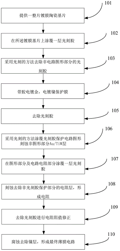
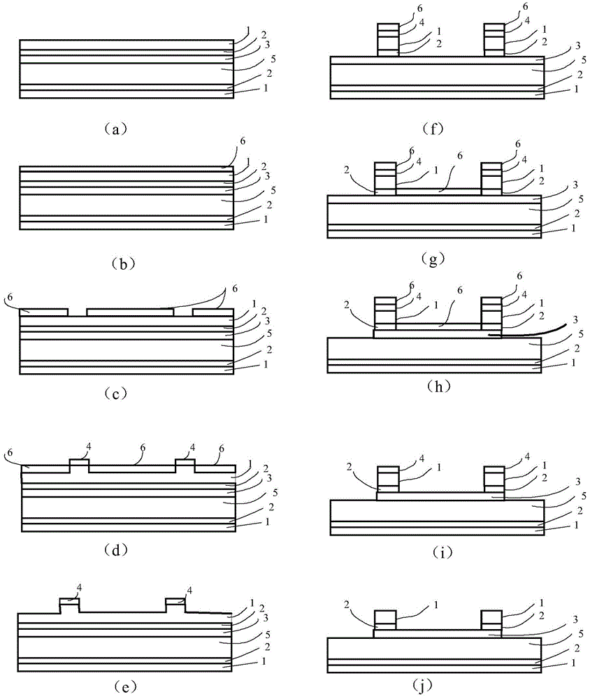
[0027] The invention provides a method for preparing a metal protective film for thin film circuit testing, which comprises the following steps:

[0028] Step 1, coating a layer of photoresist on the coated ceramic substrate, and then removing the photoresist on the non-circuit pattern part of the coated ceramic substrate by photolithography;

[0029] Step 2, performing electroplated gold and electroplated nickel protective film on the photolithographically processed said coated ceramic substrate, and then removing the remaining photoresist;

[0030] Step 3, using a photolithography method to coat the photoresist to protect the circuit pattern and etch the Au / TiW layer of the non-pattern part;

[0031] Step 4, coating a layer of photoresist on the graphic part and the circuit resistance part of the coated ceramic substrate, and etching and removing the resistance layer of the non-photoresist protected part on the coated ceramic substrate to form a resistance; and then Remove ...


PUM

PropertyMeasurementUnit
thicknessaaaaaaaaaa
thicknessaaaaaaaaaa
thicknessaaaaaaaaaa

Abstract

The invention discloses a method for manufacturing a metal protective film used for a film circuit test. The method includes the following steps that a ceramic substrate plated with a TaN / TiW / Au metal film is coated with a layer of photoresist, and the photoresist on the non-circuitous-pattern part of the ceramic substrate plated with the film is removed through a photo-etching method; a self-adhesive gold electroplated protective film and a self-adhesive nickel electroplated protective film are performed on the ceramic substrate plated with the film after photo-etching treatment, and then the photoresist is removed; the photo-etching method is adopted for performing photoresist coating to protect a circuitous pattern, and an Au / TiW layer of the non-pattern part is etched; the pattern part and circuitous resistance part of the ceramic substrate plated with the film are coated with layers of photoresist by the adoption of the photo-etching method, and a resistor layer of a non-photoresist-protection part is etched to form circuitous resistors; then, all the photoresist is removed, correction is performed on resistance values of the resistors, finally, the nickel electroplated protective film is removed through corrosion, and a film circuit is obtained. The machining steps of the nickel layer electroplating and nickel layer corroding are added, a gold strip line can be well protected from damage by a test probe through the nickel electroplated metal protective film, machining quality and the finished product rate of the film circuit are improved, and manufacturing cost of the film circuit is reduced.

Description

technical field [0001] The invention relates to the field of thin film circuit processing and production, in particular to a method for preparing a metal protective film for thin film circuit testing. Background technique [0002] Microwave thin film circuits have the advantages of high interconnection density and high line precision, and are widely used in the fields of communication and aerospace. Microwave thin film circuit processing generally needs to go through several process steps of photolithography, electroplating, scribing, and resistance adjustment. Among them, the resistance adjustment is to make the resistance value of the resistance reach the design requirement range through thermal oxidation, anodic oxidation, laser resistance adjustment and other methods. In the process of adjusting the resistance, it is necessary to use the test probe to repeatedly test the resistance value of the thin film resistor to determine whether the resistance value is adjusted in ...

Claims


Application Information

Patent Timeline
Patent Type & Authority Applications(China)
IPC IPC(8): H01L21/3205H01L21/31H01L21/32
CPCH01L21/02697H01L28/20
Inventor 王进马子腾李鸽孙毅
Owner THE 41ST INST OF CHINA ELECTRONICS TECH GRP
Why Eureka
Try Eureka