Manufacturing process of pressure sensor sensitive element
A pressure sensor and sensitive element technology, applied in electrical components, electric solid state devices, semiconductor devices, etc., to increase long-term stability, improve signal linearity, and reduce manufacturing costs
- Summary
- Abstract
- Description
- Claims
- Application Information
AI Technical Summary
Problems solved by technology
Method used
Image
Examples
Embodiment
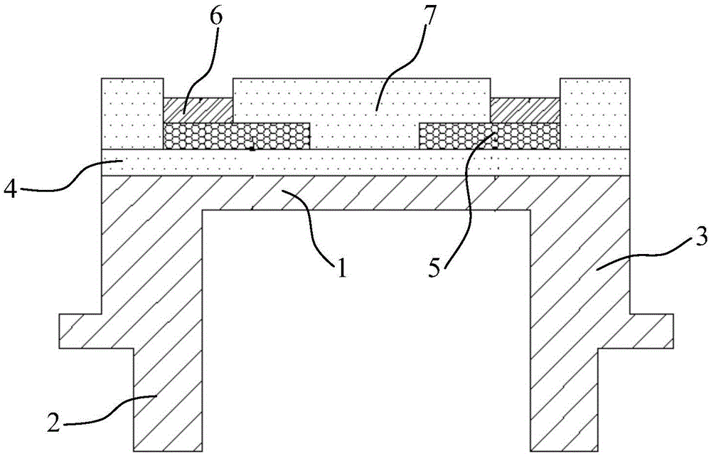
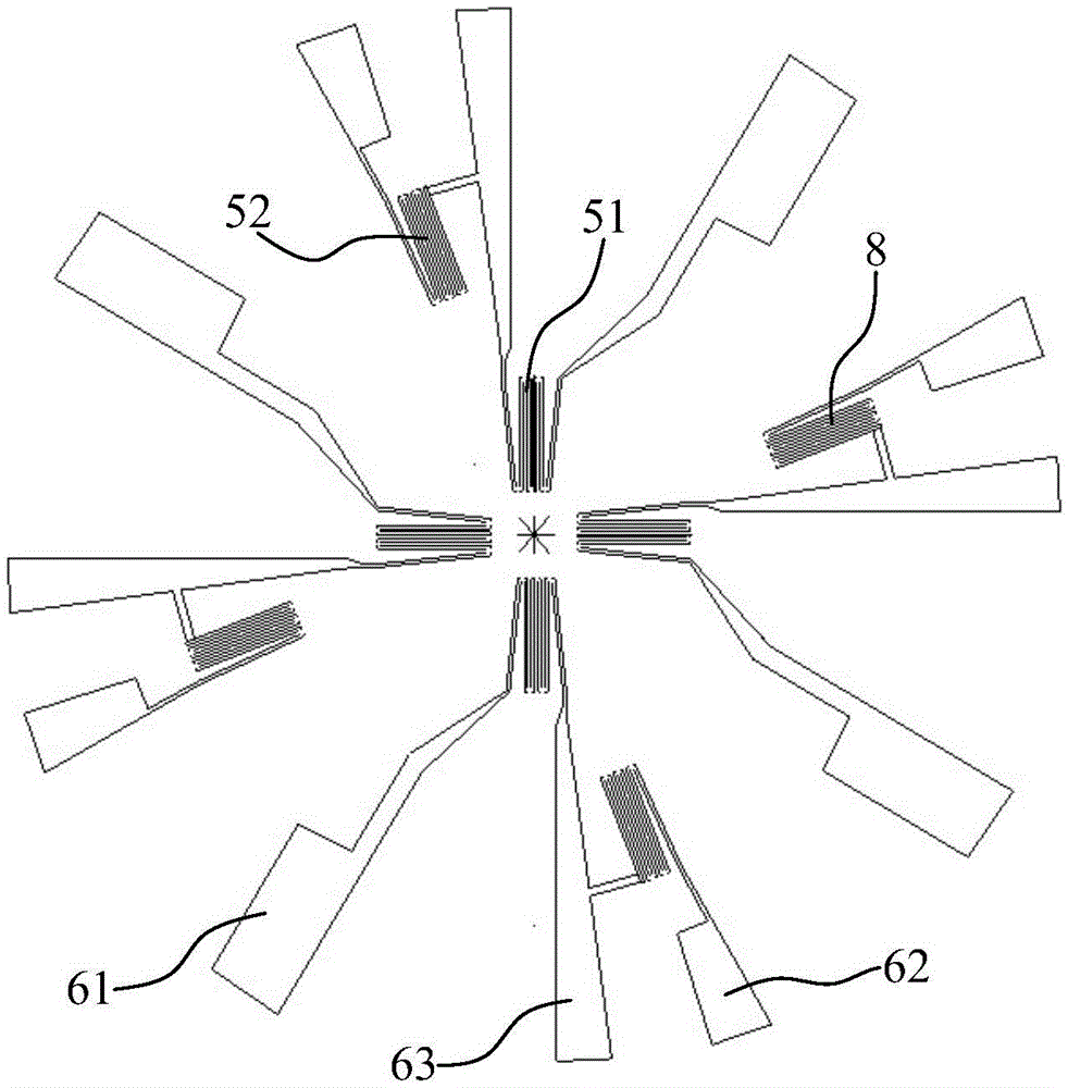
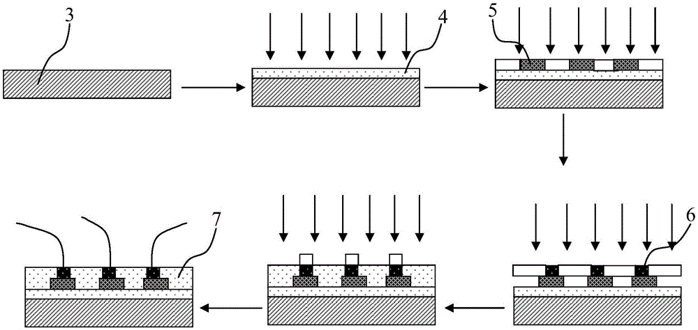
[0029] Embodiment: A manufacturing process of a pressure sensor sensitive element, the pressure sensor sensitive element includes a cup-shaped substrate 3 composed of a circular base layer 1 and an annular side plate 2 located in the circumferential direction of the circular base layer 1, located in the circular Form the silicon dioxide spacer layer 4 on the upper surface of the base layer 1, and the surface of the silicon dioxide spacer layer 4 opposite to the circular base layer 1 is provided with at least four boron-doped P-type microcrystalline silicon strips 5, and a metal electrode layer 6 Located on the surface opposite to the boron-doped P-type microcrystalline silicon strip 5 and the silicon dioxide isolation layer 4, the boron-doped P-type microcrystalline silicon strip 5 is filled with a silicon dioxide insulating layer 7; the at least four doped The boron P-type microcrystalline silicon strip 5 includes at least 2 first boron-doped P-type microcrystalline silicon st...
PUM
 Abstract
Description
Claims
Application Information


