Method for manufacturing MWT photovoltaic cell with passivated back
A manufacturing method and photovoltaic cell technology, applied in photovoltaic power generation, final product manufacturing, sustainable manufacturing/processing, etc., to achieve low transformation costs and high efficiency
- Summary
- Abstract
- Description
- Claims
- Application Information
AI Technical Summary
Problems solved by technology
Method used
Image

Examples
Embodiment 1
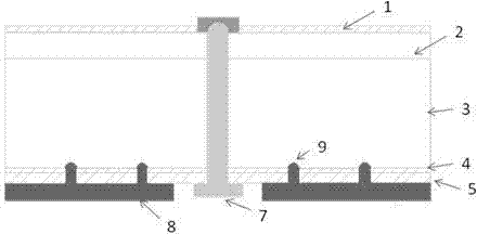
[0025] Embodiment 1: Both MWT technology and back passivation technology are two means to improve the efficiency of photovoltaic cells. In this embodiment, the two are combined to obtain a photovoltaic cell with higher conversion efficiency. First, a P-type silicon wafer 3 with a resistivity of 2 ohm·cm is selected, and the oxide and metal impurities on the surface of the silicon wafer are removed by cleaning, and at the same time, the mechanical damage layer on the surface of the silicon wafer is also removed. The surface of the cleaned silicon wafer is textured to form an undulating texture that reflects the incident light multiple times and increases the absorption of sunlight by the silicon wafer. The textured silicon wafer is placed in a diffusion tube for phosphorus diffusion to form an N-type diffusion layer 2 with a sheet resistance of 75 ohm / sq. During the diffusion process, phosphosilicate glass will be formed on the surface of the silicon wafer. After removing only ...
Embodiment 2
[0029] Embodiment 2: In this embodiment, a P-type silicon wafer 3 with a resistivity of 0.5 ohm·cm is selected for cleaning to remove oxides and metal impurities on the surface of the silicon wafer, and at the same time remove the mechanically damaged layer on the surface of the silicon wafer. The surface of the cleaned silicon wafer is textured to form an undulating texture that reflects the incident light multiple times and increases the absorption of sunlight by the silicon wafer. The textured silicon wafer is put into a diffusion tube for phosphorus diffusion to form an N-type diffusion layer 2 with a sheet resistance of 30 ohm / sq. During the diffusion process, phosphosilicate glass will be formed on the surface of the silicon wafer. After removing the phosphosilicate glass on the surface of the silicon wafer, the polishing machine will perform single-sided polishing on the back under the protection of water film or weather isolation acid mist.
[0030] A layer of aluminum...
Embodiment 3
[0033] Embodiment 3: In this embodiment, a P-type silicon wafer 3 with a resistivity of 6 ohm·cm is selected, and the oxide and metal impurities on the surface of the silicon wafer are cleaned to remove the mechanical damage layer on the surface of the silicon wafer. The surface of the cleaned silicon wafer is textured to form an undulating texture that reflects the incident light multiple times and increases the absorption of sunlight by the silicon wafer. The textured silicon wafer is put into a diffusion tube for phosphorus diffusion to form an N-type diffusion layer 2 with a sheet resistance of 120 ohm / sq.
[0034] A layer of aluminum oxide layer 4 with a thickness of 100 nm was deposited on the polished backside of the silicon wafer by plasma enhanced chemical vapor deposition (PECVD) as a backside passivation layer. A through hole in the form of 4×4 is drilled on the silicon wafer with a red laser, the diameter of the through hole is 1000um, and the hole pitch is 100mm. ...
PUM
 Abstract
Description
Claims
Application Information