LED (light emitting diode) structure and manufacturing method thereof

A technology of LED structure and manufacturing method, which is applied in the direction of electrical components, circuits, semiconductor devices, etc., can solve the problems of consuming large metal organic compound sources, increasing device costs, and rising chip costs, so as to save metal organic compound sources and reduce growth. Time, application of a wide range of effects

Inactive Publication Date: 2014-03-26
HANGZHOU SILAN AZURE
View PDF6 Cites 4 Cited by
  • Summary
  • Abstract
  • Description
  • Claims
  • Application Information

AI Technical Summary

Problems solved by technology

Although the vertical structure LED chip obtained by silicon substrate transfer has many advantages, the cost of the chip will increase
[0005] In addition, the use of sapphire substrates requires additional patterned substrate processes, which will also increase device costs
[0006] In addition, the thickness of the epitaxial layer in the current LED light-emitting structure is basically 5-7 μm. For such a thickness, it takes 7-9 hours to grow in conventional MOCVD equipment. Such a long time requires a large amount of metal-organic compound sources. leading to an increase in the cost of chips

Method used


Image

  • LED (light emitting diode) structure and manufacturing method thereof
  • LED (light emitting diode) structure and manufacturing method thereof
  • LED (light emitting diode) structure and manufacturing method thereof

Examples


no. 1 example

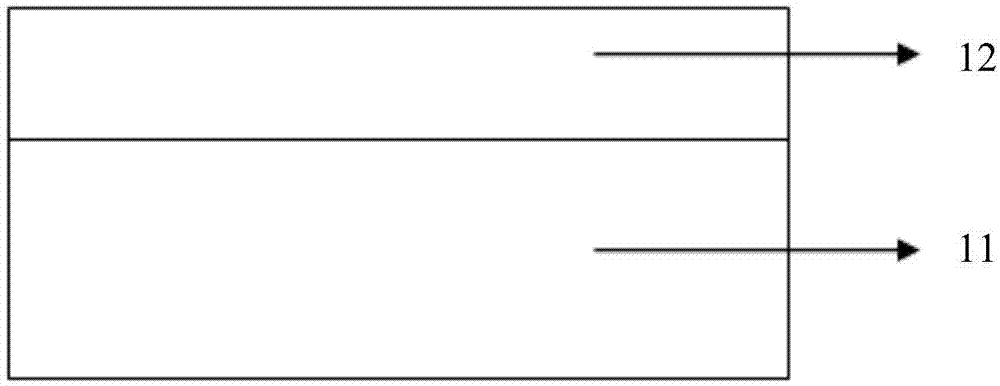
[0056] refer to figure 2 A substrate 11 is provided. As a non-limiting example, the substrate 11 in this embodiment is a silicon substrate, for example, a 2-8 inch silicon substrate.

[0057] After that, the reflective layer 12 is formed on the surface of the substrate 11 . The reflective layer 12 is preferably a Bragg reflector structure, for example, silicon oxide (SiO2) can be formed by evaporation or sputtering. 2 ) and titanium oxide (TiO 2 ) periodic structure, that is, the Bragg mirror structure. Preferably, ion-assisted evaporation can be used to deposit SiO 2 and TiO 2 cycle structure. By adjusting the film thickness, the reflection rate of the formed reflective layer 12 between 440-550 nm wavelength can be higher than 95%, and its thickness range is preferably 0.1-100 μm, more preferably 2-3 μm.

[0058] For example, in this embodiment, the period of the Bragg reflector is 28 periods, and its thickness is about 2.13um.

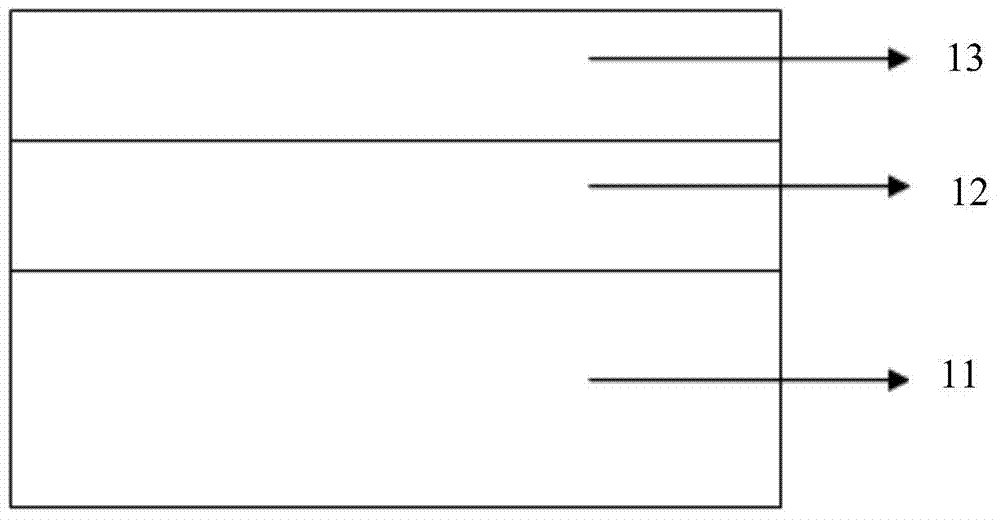
[0059] refer to image 3 , forming an...

no. 2 example

[0070] refer to figure 2 , a substrate 11 is provided, and the substrate 11 in this embodiment is a sapphire substrate. A reflective layer 12 is then formed on the substrate 11 . Please refer to the first embodiment for the material, structure, and formation process of the reflective layer 12 , which will not be repeated here.

[0071] refer to image 3 , forming an AlN buffer layer 13 on the reflective layer 12 . In the second embodiment, the method of forming AlN is still the radio frequency magnetron sputtering method, but the AlN target is not used to react to form AlN, but the AlN target is directly sputtered to obtain the AlN buffer layer 13 with a preferred orientation. The specific process conditions are: the working pressure is 2.0Pa, the power is 300W, the temperature is 370°C, and the sputtering atmosphere is N 2 The concentration of 99.99%.

[0072] refer to Figure 4 , the LED light emitting structure 17 is deposited on the AlN buffer layer 13 by MOCVD meth...


PUM


Abstract

The invention provides an LED (light emitting diode) structure and a manufacturing method thereof. The LED structure comprises a substrate, a reflecting layer and an LED luminescent structure, wherein the reflecting layer covers the substrate; the LED luminescent structure is arranged on the reflecting layer, the LED luminescent structure comprises an upper semiconductor layer, a lower semiconductor layer and a multiple-quantum-well layer which is arranged between the upper semiconductor layer and the lower semiconductor layer, one of the upper semiconductor layer and the lower semiconductor layer is P-type doped and the other one is N-type doped. By adopting the LED structure, the light absorption problem can be overcome without transferring or schematizing the substrate, so that the manufacturing cost is reduced; moreover, the growth time for adopting the MOCVD (metal organic chemical vapor deposition) to form the LED luminescent structure can be reduced.

Description

technical field [0001] The invention relates to the technical field of semiconductor optoelectronic chips, in particular to an LED structure and a manufacturing method thereof. Background technique [0002] Semiconductor light-emitting diode (LED) is a new type of solid-state cold light source. It has many advantages such as high energy efficiency, long life, small size, and low voltage. It is widely used in people's daily life, such as traffic lights, headlights, outdoor displays, mobile phone backlight , LEDs are widely used in electrical indicator lights and some lighting street lights. In particular, in terms of energy saving and environmental protection, LED lamps have obvious advantages over ordinary incandescent lamps and fluorescent lamps. Therefore, it has become a consensus that LED light sources will replace traditional light sources as the main lighting source in the future. [0003] However, to replace traditional light sources, the cost of LEDs should be as lo...

Claims


Application Information

Patent Timeline
Patent Type & Authority Applications(China)
IPC IPC(8): H01L33/10H01L33/12H01L33/00
CPCH01L33/10H01L33/005H01L33/12
Inventor 张昊翔封飞飞万远涛李东昇江忠永
Owner HANGZHOU SILAN AZURE
Why Eureka
Try Eureka